
Data processing device

a data processing device and data processing technology, applied in the field of large-scale integrated circuits, can solve the problems of increasing the cost, affecting the smooth display of moving pictures, and often arising performance bugs beyond the anticipation of programmers, so as to improve the performance of data processing devices

Inactive Publication Date: 2006-03-16
RENESAS TECH CORP
View PDF1 Cites 7 Cited by
  • Summary
  • Abstract
  • Description
  • Claims
  • Application Information

AI Technical Summary

Benefits of technology

[0017] The invention enables data process

Problems solved by technology

Where many circuit modules are incorporated into a single LSI, performance bugs beyond the anticipation of programmers often arise.
In a typical example of this problem, access requests from different circuits concentrate on a bus that connects circuit modules in the chip, making it impossible to secure a transfer band required by moving pictures and therefore to display the moving pictures smoothly.
If the bus width or the parallelism of arithmetic processors is increased to be sufficient for the highest expected level of performance requirement, such a physical abundance policy would boost the cost and accordingly invite an economic f

Method used


Image

  • Data processing device
  • Data processing device
  • Data processing device

Examples


first embodiment

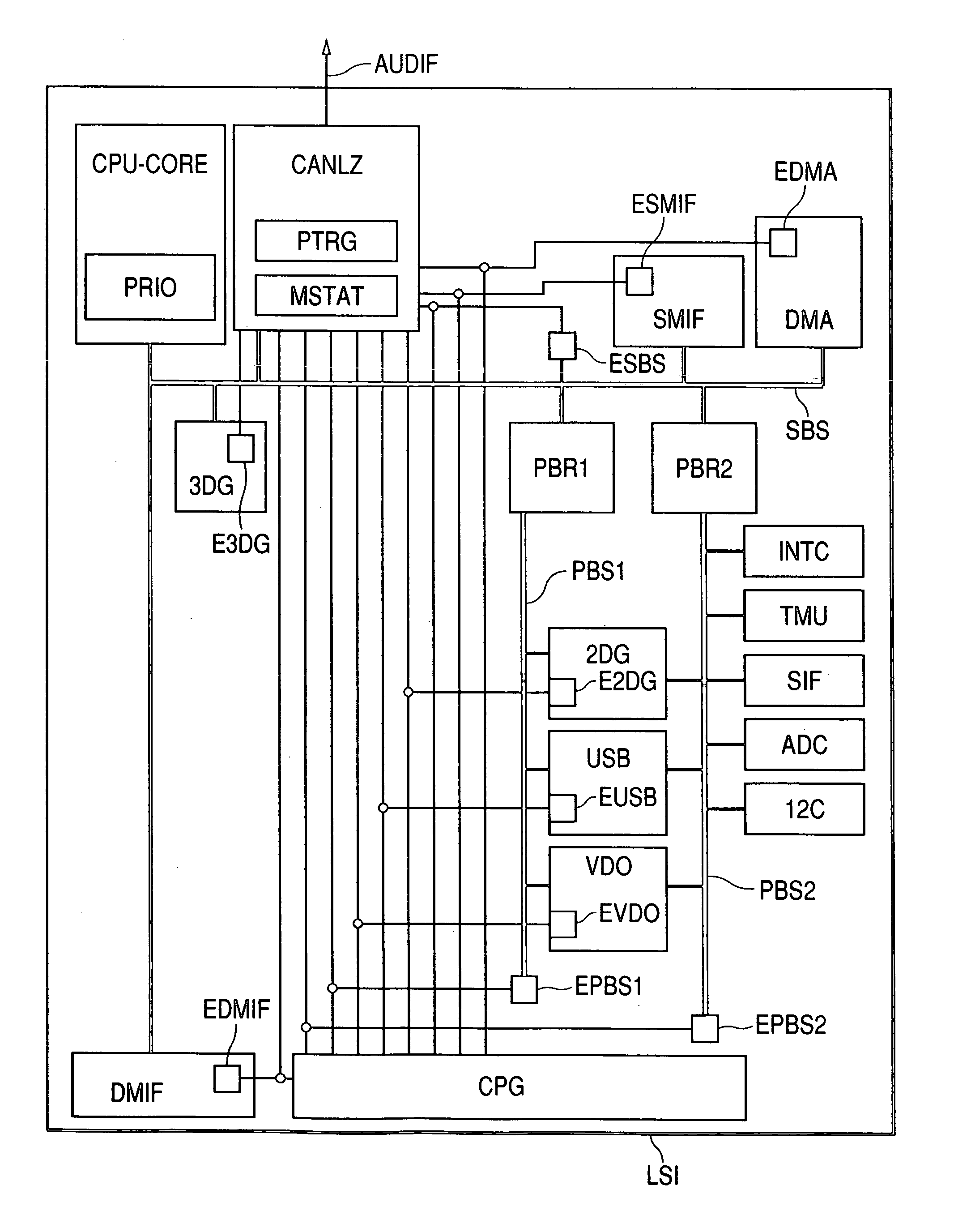
[0033]FIG. 1 shows the configuration of a data processing device equipped with an observation block according to the invention. The data processing device according to the invention is, though not limited to, an LSI formed over a single semiconductor substrate. As shown in FIG. 1, this LSI includes a CPU core (CPU-CORE), a system bus SBS, a bus bridge PBR1 for performing protocol exchanges between this system bus SBS and a peripheral bus PBS1, a bus bridge PBR2 for performing protocol exchanges between the system bus SBS and a peripheral bus PBS2, a direct memory access controller DMA for transferring data on the system bus without passing the CPU core, a DRAM interface controller DMIF, an SRAM / ROM interface controller SMIF, a 3D graphics accelerator 3DG, a 2D graphics accelerator 2DG, a USB interface controller USB, a video interface controller VDO, a clock controller CPG, an interrupt controller INTC and other peripheral circuits.

[0034] Besides these circuits, every one of the ci...

second embodiment

[0052] This embodiment has a status referencing circuit MSTAT to enable the state of each observation object circuit obtained from the observation blocks to be referenced from the CPU core as shown in FIG. 1.

[0053]FIG. 4 shows an example of MSTAT. MSTAT is packaged as a 32-bit register, and each bit of the register show whether or not the pertinent module is usable. Information on whether or not each package is in a usable state is conveyed by way of a STAT signal connected from each of the status observation blocks ESBS, EPBS1, EPBS2, ESMIF, EDMIF, EUSB, E3DG, E2DG and EDMA in FIG. 1 to MSTAT. For instance, bits 0 and 1 for the status referencing circuit MSTAT indicate whether or not the DRAM interface controller DMIF is usable. In other words, it indicates the state of the command queue DMQ which DMIF has. If this value is 0, an entirely unoccupied state is indicated, or if it is 1 or above, it means that processing is already booked for, and the issuance of any more processing r...

third embodiment

[0058]FIG. 5 shows a mechanism for feeding back information from an observation block for system bus ESBS on the system bus SBS and a bus observation block EPBS on the peripheral bus PBS to the clock controller CPG. ESBSS and EPBSS are information conveying signals from the respective observation blocks. The clock controller CPG is equipped inside with a frequency divider DIV which divides the frequency of the reference clock, and supplies its clocks to individual circuits. In this embodiment, it supplies a clock SCK to the system bus SBS and a clock PCK to the peripheral bus PBS. The clock controller CPG knows bus statuses from the ESBSS and EPBSS signals, dynamically alters the division ratio setting to match the states, and accordingly alters the clocks to be supplied to these bus circuits. These localized frequency alterations can raise the operating frequency in only the needed part, and thereby allows optimization in both power and processing speed aspects. Moreover, as the fr...


PUM


Abstract

A data processing device which, even if congestion occurs on a bus circuit of a specific processing circuit in an LSI in which multiple circuit modules are connected by buses, can fully actualize the performance potential of the system on chip. Buses and slave circuits on which accesses concentrate are provided with observation blocks. Each observation block has a mechanism to notify system control circuits such as a clock controller and master circuits such as CPU cores of the acquired status information, and each master circuit further has a mechanism capable of dynamically altering the priority order for notifying the bus circuits and slave circuits of the priority order of processing.

Description

CLAIM OF PRIORITY [0001] The present application claims priority from Japanese application JP 2004-263313 filed on Sep. 10, 2004, the content of which is hereby incorporated by reference into this application. FIELD OF THE INVENTION [0002] The present invention relates to a large-scale integrated circuit (LSI) having observation blocks for observing the status of the system, and more particularly to a data processing device provided with observation blocks to be formed over a semiconductor substrate. The LSI to which the invention relates here is an LSI chip containing arithmetic and processing circuits including a central processing unit (CPU) and a digital signal processor (DSP) and an interface with memory circuits including a synchronous DRAM (SDRAM). BACKGROUND OF THE INVENTION [0003] Along with the increase in the integrating scale of LSIs, the main use of LSIs has shifted from CPUs alone to system-on-chips (SOCs), and the trend to require LSIs to have a high level of system p...

Claims


Application Information

Patent Timeline
IPC IPC(8): G06F13/36
CPCG06F13/364
Inventor SAEN, MAKOTOSUZUKI, KEI
Owner RENESAS TECH CORP
Features
  • Generate Ideas
  • Intellectual Property
  • Life Sciences
  • Materials
  • Tech Scout
  • Unparalleled Data Quality
  • Higher Quality Content
  • 60% Fewer Hallucinations
Learn More