Power semiconductor module and method of manufacturing the same

a technology of semiconductor modules and semiconductor components, applied in the direction of basic electric elements, dc-ac conversion without reversal, electrical apparatus contruction details, etc., can solve the problems of limited current capacity of modules, difficult to bond metal wires by ultrasonic bonding or welding, and long time to bond metal wires. , to achieve the effect of strengthening the adhesion of thermosetting resin

Active Publication Date: 2006-03-23
FUJI ELECTRIC CO LTD
View PDF6 Cites 40 Cited by
  • Summary
  • Abstract
  • Description
  • Claims
  • Application Information

AI Technical Summary

Benefits of technology

[0011] The terminal casing can have at least one protrusion protruding toward the insulating circuit board in the bonding areas between the terminal casing and the insulating circuit board, to enable the thermosetting resin to flow

Problems solved by technology

Since the cross sectional area of the metal wires connecting the outer leads and the semiconductor chips in the power semiconductor module described above is relatively small, the module is limited in its current capacity.
While a thick metal wire can impr

Method used


Image

  • Power semiconductor module and method of manufacturing the same
  • Power semiconductor module and method of manufacturing the same
  • Power semiconductor module and method of manufacturing the same

Examples


first embodiment

[0070] Now the method for manufacturing the power semiconductor module will be described in detail below. FIG. 5 is a flow chart describing the steps for manufacturing the power semiconductor module according to the FIGS. 6(A)-14 illustrate the manufacturing steps. In the following, the manufacturing process is described in the descending order of the step numbers (S11 through S37) described in FIG. 5.

[0071] First, semiconductor chips 8 are formed (step S11). See FIG. 6(A)-6(B). In detail, IGBTs, free-wheel diodes (FWDs) and such power semiconductor devices are formed on a predetermined semiconductor substrate. Polyimide layers 42 are formed on the surfaces of the power semiconductor devices except the electrode surfaces thereof. Nickel (Ni) plating layers 43 are formed on the respective electrodes of the power semiconductor devices by electroless plating. Gold (Au) plating layers 44 are formed on the Ni plating layers 43 by electroless plating. Then, the semiconductor substrate is...

second embodiment

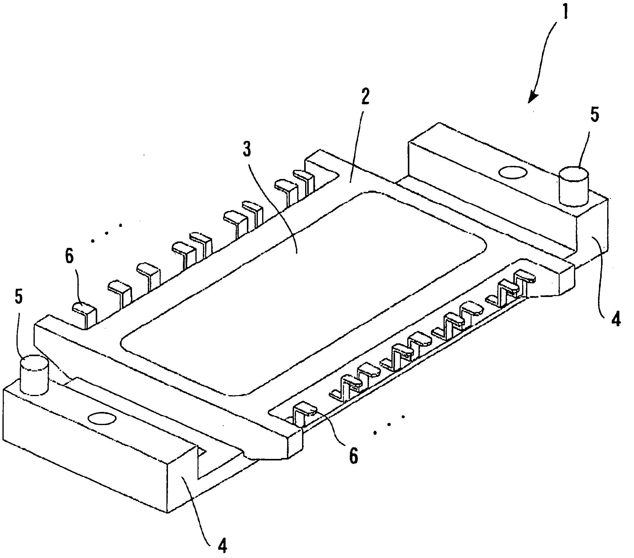
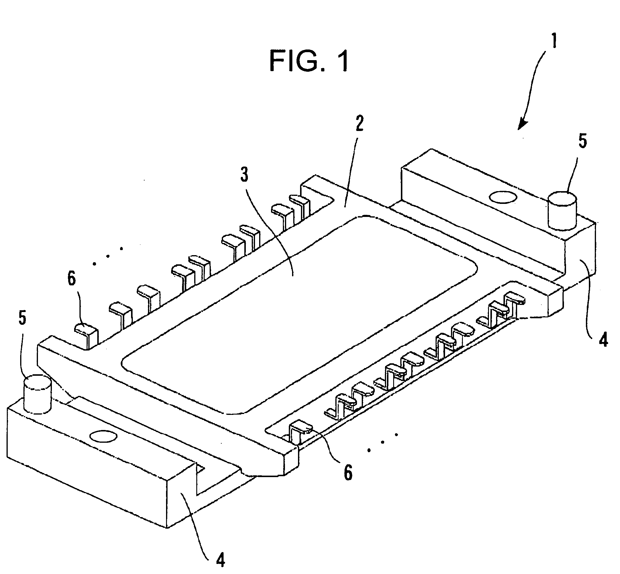
[0083] Referring to FIG. 14, the power semiconductor module 201 mounts thereon an insulating circuit board 207 including an insulating ceramic substrate 211 made of aluminum oxide (AL2O3), aluminum nitride (AlN), silicon nitride (SiN), and such ceramics. A radiator plane 212 can be formed on the lower surface of the insulating ceramic substrate 211 by laminating copper foils thereon. Copper foil patterns 213 can be formed on the upper surface of the insulating ceramic substrate 211. Semiconductor chips 8 can be surface-mounted on the copper foil patterns 213 via the solder layers 29. The protrusions 14 on the terminal casing 2 can be brought into contact with the ceramic substrate 211.

[0084] The Ni plating layers 43 and the Au plating layers 44 can be formed on the electrodes of the power semiconductor chips 8 by electroless plating to improve the solder wetness as in the second embodiment, as described with reference to FIGS. 6(A) and 6(B). Alternatively, the Ni layers and the Au l...


PUM


Abstract

A power semiconductor module and a method of manufacture thereof includes lead a frame carrying lead having inner and outer lead portions. The outer lead portions, which are connected by soldering to semiconductor chips simultaneously, eliminate the need for using bonding wires. Since no bonding wire is used for connecting the leads and the semiconductor chips, a sufficient current capacity is obtained. The bonding between an insulating circuit board and the semiconductor chips and the bonding between the semiconductor chips and the leads can be made simultaneously in a single step of reflow-soldering. As a result, the mounting time can be shortened and the power semiconductor module can be manufactured more efficiently.

Description

BACKGROUND [0001] Power semiconductor modules are used in inverters, uninterruptive power supplies, machine tools, industrial robots, and such apparatuses in the form of packages, independent from these industrial apparatuses. Such a power semiconductor module houses therein one or more semiconductor chips insulated gate bipolar transistors (hereinafter referred to as “IGBTs”) and such power semiconductor devices constituting the power converter circuit. The power semiconductor module is mounted on a predetermined control circuit board for controlling any of the apparatuses described above. See for instance JP 2002-50722 A. [0002] The following describes such a power semiconductor module that houses a plurality of semiconductor chips. Typically, the power semiconductor module mounts the semiconductor chips on an insulating circuit board by soldering. The power semiconductor module has the leads connected to the control circuit board and the semiconductor chips by wire bonding using ...

Claims


Application Information

Patent Timeline
IPC IPC(8): H01L23/48H01L25/07H01L25/18H02M7/48
CPCH01L23/49861H01L25/072H01L2224/32225H01L2924/1305H01L2924/13055H01L2924/00
Inventor IKAWA, OSAMUMOCHIZUKI, EIJISOUTOME, MASAYUKIARIKAWA, NORIO
Owner FUJI ELECTRIC CO LTD
Why Eureka
Try Eureka