Electro-optical device, method of manufacturing the same, and electronic apparatus

a technology of electro-optical material and electronic apparatus, applied in non-linear optics, instruments, optics, etc., can solve problems such as alignment defects in liquid crystal materials, and achieve the effects of reducing alignment defects of electro-optical materials caused by the step of insulating layer, preventing alignment defects, and enhancing image display characteristics

Inactive Publication Date: 2006-03-23
SEIKO EPSON CORP
View PDF19 Cites 29 Cited by
  • Summary
  • Abstract
  • Description
  • Claims
  • Application Information

AI Technical Summary

Benefits of technology

[0009] An advantage of the invention is that it provides an electro-optical device in which the number of sides of a step of an insulating layer included in one pixel is reduced, thereby preventing alignment defects from occurring. Another advantage of the invention is that it provides a method of manufacturing such an electro-optical device and an electronic apparatus having such an electro-optical device.
[0010] According to a first aspect of the invention, an electro-optical device includes a pair of substrates with an electro-optical material layer interposed therebetween, and a plurality of pixels, each having a reflection region and a transmission region. The reflection regions are disposed on opposing sides of adjacent pixels. On one substrate of the pair of substrates, an insulating layer is formed in the reflection region, such that the thicknesses of the electro-optical material layer in the reflection region and the transmission region are made different from each other. Further, the insulating layer is formed across two adjacent pixels along a direction in which the reflection regions of adjacent pixels continue.
[0011] That is, by adjusting the thickness of the electro-optical material layer to reduce the thickness of the electro-optical material layer in the reflection region, the insulating layer is formed across two adjacent pixels along a predetermined direction, such that the step of the insulating layer included in one pixel can be reduced. Therefore, retardation is optimized in the reflection region and the transmission region, respectively. Further, it is possible to provide an electro-optical device in which alignment defects of the electro-optical material caused by the step of the insulating layer are reduced and display characteristics of an image to be displayed can be enhanced.
[0012] In the electro-optical device according to the first aspect of the invention, it is preferable that the insulating layer be formed in a stripe shape across the pixels that are arranged along a direction orthogonal to the direction in which the reflection regions of adjacent pixels continue.
[0013] According to this configuration, the step, which is formed along the predetermined direction in the insulating layer, can be removed. Therefore, the step of the insulating layer included in one pixel can be further reduced, such that display characteristics can be further enhanced.
[0014] In the electro-optical device according to the first aspect of the invention, it is preferable that the step of the insulating layer be formed in a tapered shape.

Problems solved by technology

This step can cause alignment defects in a liquid crystal material.

Method used


Image

  • Electro-optical device, method of manufacturing the same, and electronic apparatus
  • Electro-optical device, method of manufacturing the same, and electronic apparatus
  • Electro-optical device, method of manufacturing the same, and electronic apparatus

Examples


first embodiment

[0081] A first embodiment of the invention relates to an electro-optical device including a pair of substrates with an electro-optical material layer interposed therebetween, and a plurality of pixels, each having a reflection region and a transmission region. The reflection regions are formed on opposing sides of adjacent pixels. On one substrate of the pair of substrates, an insulating layer is formed in at least the reflection region, such that the thicknesses of the electro-optical material layer in the reflection region and the transmission region are made different from each other. The insulating layer is formed across two adjacent pixels along a direction in which the reflection regions of adjacent pixels continue.

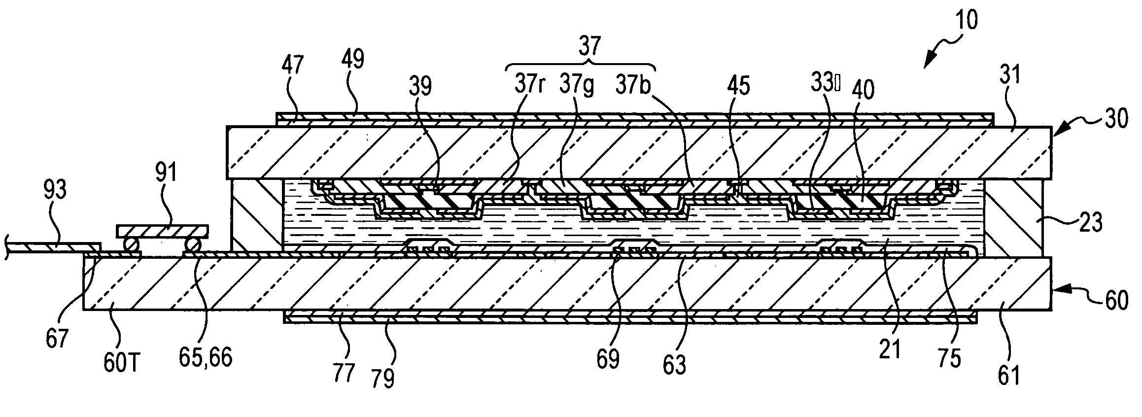
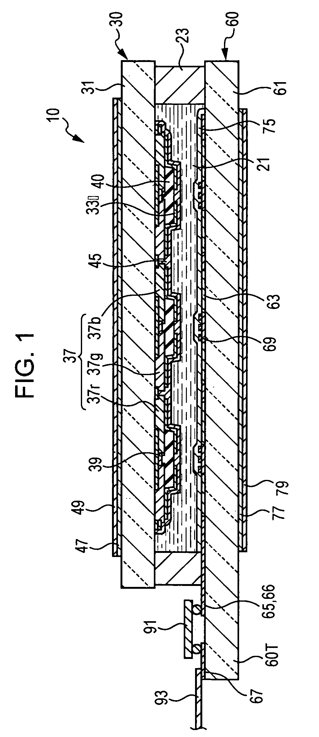
[0082] Hereinafter, the electro-optical device according to the first embodiment of the invention will be described with reference to FIGS. 1 to 10C by way of a liquid crystal device that has a color filter substrate 30 with a predetermined insulating layer 40 form...

second embodiment

[0136] A second embodiment of the invention relates to a method of manufacturing an electro-optical device having a pair of substrates with an electro-optical material layer interposed therebetween and a plurality of pixels, each having a reflection region and a transmission region. The method of manufacturing an electro-optical device includes forming a light reflecting film on a substrate, such that the reflection regions are formed on opposing sides of adjacent pixels, and forming an insulating layer in at least the reflection region such that the thicknesses of the electro-optical material layer in the reflection region and the transmission region are made different from each other. Here, the insulating layer is formed across two adjacent pixels along a direction in which the reflection regions of the adjacent pixels continue.

[0137] Hereinafter, as an example of the method of manufacturing an electro-optical device according to the second embodiment, a method of manufacturing a...

third embodiment

[0153] In the third embodiment, the transflective electro-optical device of the first embodiment is applied to an active-matrix-type liquid crystal display device using TFT elements (Thin Film Transistors), which are three-terminal active elements, as switching elements.

[0154]FIG. 14A is a cross-sectional view showing a liquid crystal display device 210 according to the third embodiment, and FIG. 14B is a plan view showing the liquid crystal display device 210. As shown in FIG. 14A, a counter substrate 230 and an element substrate 260 are bonded to each other in the peripheral portions thereof with a sealing material and a liquid crystal material is injected into a gap which is surrounded by the counter substrate 230, the element substrate 260, and the sealing material, such that the liquid crystal display device 210 is formed.

[0155] In addition, the counter substrate 230 made of glass, plastic, or the like includes a color filter, that is, a colored layer 237, a counter electrode...


PUM

PropertyMeasurementUnit
electro-opticalaaaaaaaaaa
thicknessaaaaaaaaaa
reflectionaaaaaaaaaa

Abstract

An electro-optical device includes a pair of substrates with an electro-optical material layer interposed therebetween, and a plurality of pixels, each having a reflection region and a transmission region. The reflection regions are disposed on opposing sides of adjacent pixels. On one substrate of the pair of substrates, an insulating layer is formed in the reflection region, such that the thicknesses of the electro-optical material layer in the reflection region and the transmission region are made different from each other. Further, the insulating layer is formed across two adjacent pixels along a direction in which the reflection regions of adjacent pixels continue.

Description

BACKGROUND OF THE INVENTION [0001] 1. Technical Field [0002] The present invention relates to an electro-optical device, to a method of manufacturing such an electro-optical device, and to an electronic apparatus. More particularly, the present invention relates to an electro-optical device in which alignment defects caused by multi-gap steps are reduced, to a method of manufacturing such an electro-optical device, and to an electronic apparatus having such an electro-optical device. [0003] 2. Related Art [0004] Conventionally, as image display devices, liquid crystal display devices have been widely used. In the liquid crystal display devices, a pair of substrates are disposed to face each other, each substrate having electrodes formed thereon. Then, when a voltage to be applied to a plurality of pixels which are intersections between the electrodes is selectively turned on and off, light passing through a liquid crystal material of a pixel region is modulated, such that an image, ...

Claims


Application Information

Patent Timeline
Patent Type & Authority Applications(United States)
IPC IPC(8): G02F1/1335
CPCG02F1/133555
Inventor YAMAGUCHI, YOSHIOKURASHIMA, TAKESHI
Owner SEIKO EPSON CORP
Why Eureka
Try Eureka