[0026] An
advantage of the invention is to provide a
semiconductor memory device that can solve the above problems in the
conventional technique and increase the number of pieces of data to be read with a single read command and the number of pieces of data to be written with a single write command without increasing the number of read amplifiers and write drivers.
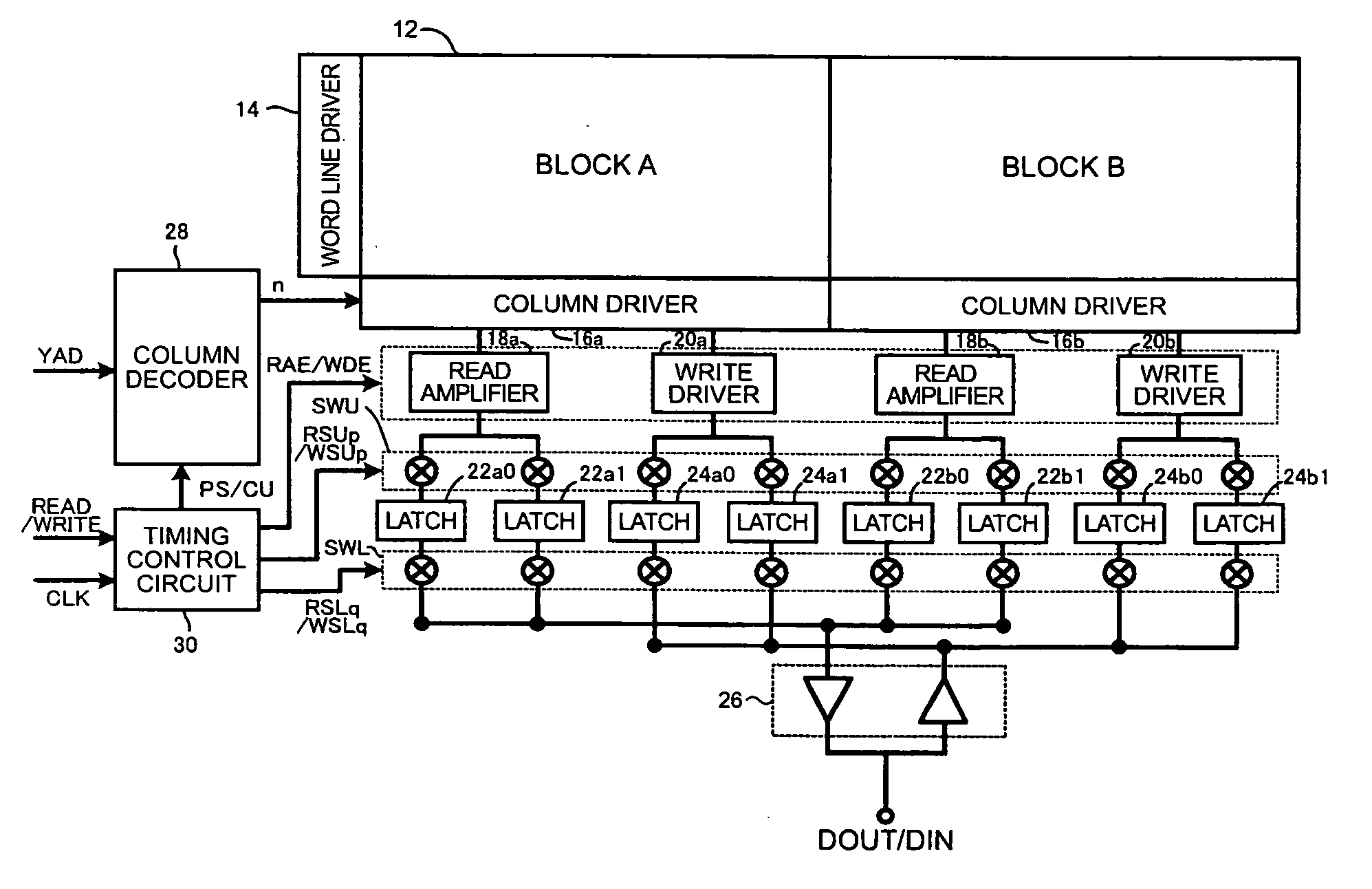
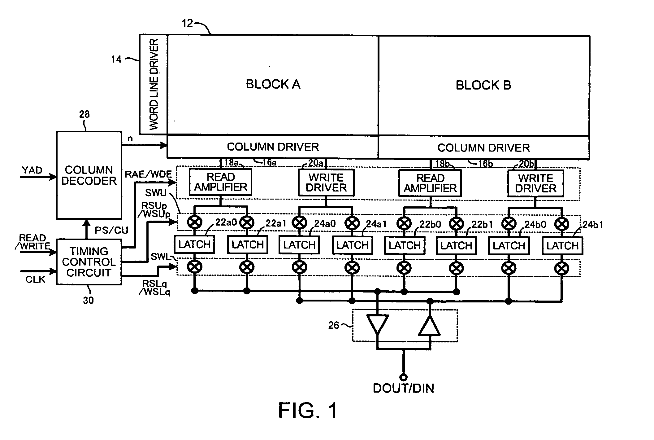
[0027] According to a first aspect of the invention, a semiconductor memory device includes: a plurality of memory cells arranged in a matrix; a memory cell array divided into a plurality of blocks; a plurality of read amplifiers, each of which is coupled correspondingly to each of the blocks; and a plurality of latch circuits, each group of which is coupled correspondingly to each of the read amplifiers and includes two or more latch circuits coupled to one another in parallel. In order to read a plurality of data consecutively from the memory cell array of the above semiconductor memory device, the data are firstly read from one desired memory cell for each block. Secondly, the read data are inputted and latched, via the read amplifier corresponding to the same block, to one of the latch circuits included in a group of latch circuits corresponding to the same read amplifier. Thirdly, the data are read from another desired memory cell, which is different from the memory cell from which the data are formerly read, for each block. Fourthly, the read data are inputted and latched, via the read amplifier corresponding to the same block, to one of the latch circuits, which is different from the latch circuit to which the data are formerly latched, included in the group of latch circuits corresponding to the same read amplifier. Lastly, the latched data are outputted in a desired order from each of the latch circuits having the latched data.
[0028] As described above, in the semiconductor memory device according to the first aspect of the invention, by
coupling a group of two or more latch circuits to each read amplifier, the number of pieces of data to be read with a single read command can be increased without increasing the number of read amplifiers. This is because, even if only a single read amplifier is coupled to each block, two or more pieces of data can be read consecutively from each block via each read amplifier.
[0029] In the semiconductor memory device according to the first aspect of the invention, it is preferable that if a desired value is inputted from outside as a column address value, the data that are latched to each of the latch circuits are data that are read from the memory cells of consecutive column address values starting from the desired value.
[0030] By employing the above configuration, data can be read consecutively from each of the memory cells of consecutive column address values starting from the desired inputted value.
[0031] Further, according to a second aspect of the invention, a semiconductor memory device includes: a plurality of memory cells arranged in a matrix; a memory cell array divided into a plurality of blocks; a plurality of write drivers, each of which is coupled correspondingly to each of the blocks; and a plurality of latch circuits, each group of which is coupled correspondingly to each of the write drivers and includes two or more latch circuits coupled to one another in parallel. In order to write a plurality of data consecutively into the memory cell array of the above semiconductor memory device, the plurality of data are firstly inputted and latched to the plurality of latch circuits in a desired order. Secondly, the latched data are outputted, for each group of latch circuits, from one of the latch circuits included in the same group. Thirdly, the outputted data are written, via the write driver corresponding to the same group, into a desired memory cell of the block corresponding to the same write driver. Fourthly, the latched data are outputted, for each group of latch circuits, from another latch circuit included in the same group, other than the latch circuit from which the data are formerly outputted. Lastly, the outputted data are written, via the write driver corresponding to the same group, into another desired memory cell, which is different from the memory cell into which the data are formerly written, included in the block corresponding to the same write driver.

