Blue luminescent polymer and organoelectroluminescent device using the same
a luminescent polymer and organoelectroluminescent technology, applied in the direction of discharge tube luminescnet screens, other domestic articles, natural mineral layered products, etc., can solve the problems of low quantum efficiency, low color purity, crystallization of thin films, etc., to improve color coordinate characteristics in the blue range, high charge mobility, good structural stability
- Summary
- Abstract
- Description
- Claims
- Application Information
AI Technical Summary
Benefits of technology
Problems solved by technology
Method used
Image
Examples
preparation example 1
Manufacturing a Polymer Represented by Formula 4
[0097]
A) Preparation of 2-bromo-9,9′-dioctylfluorene (A′)
[0098] 24.5 g of 2-bromofluorene (100 mmol) was dissolved in 200 ml of dimethylsulfoxide (DMSO), and then 14.5 g of KOH (259 mmol) was added thereto. The result was stirred for 20 minutes. 42.5 g of bromooctane (220 mmol) was added to the stirred mixture, and then stirred at room temperature for 16 hours.
[0099] After the reaction was completed, 300 ml of distilled water was added to the reaction mixture, and then extracted using chloroform to concentrate the mixture. This concentrated result was column-chromatographed using hexane as an eluent to produce 46.9 g of 2-bromo-9,9′-dioctylfluorene (A′) (yield: 94%).
B) Preparation of 9,9′-dioctylfluorenyl-2-boronic acid (B′)
[0100] 40.8 g of 2-bromo-9,9′-dioctylfluorene(A′) (87 mmol) was dissolved in 150 ml of anhydrous tetrahydrofuran (THF). 2.11 g of Mg (86.8 mmol) and a trace of I2 were added to the result, and then refluxed for ...
example 1
Manufacturing an Organic EL Device
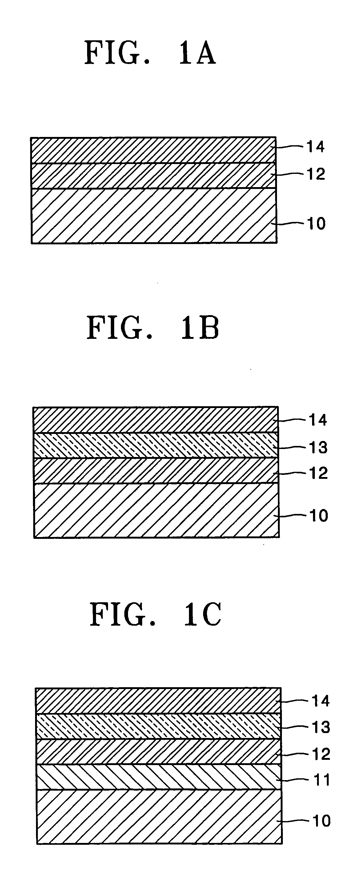
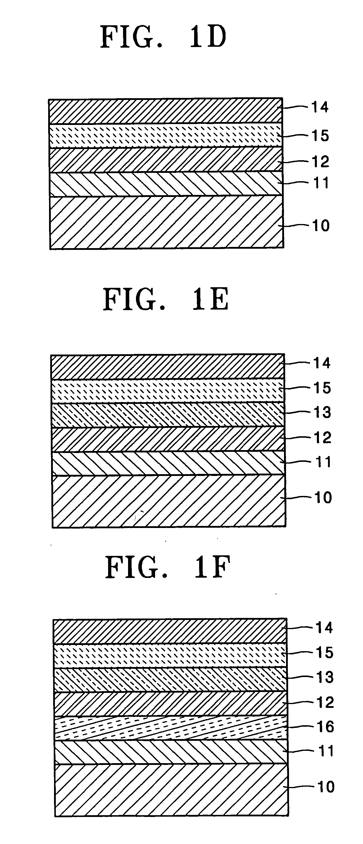
[0115] An organic EL device was manufactured using the polymer represented by Formula 4 prepared in Preparation Example 1.
[0116] First, indium-tin oxide (ITO) was coated on a transparent glass substrate. The ITO layer was patterned in a desirable form using a photosensitive resin and etchant, and then cleaned. Then, Batron P 4083 (obtained from Bayer Co.) was coated on the ITO layer to form a conducting buffer layer. The conducting buffer layer had a thickness of 800 Å. The result was baked at 180° C. for one hour. Then, 1 part by weight of the polymer represented by Formula 4 was dissolved in 99 parts by weight of toluene to prepare a composition for forming an emission layer. In order to form a polymer thin film, the buffer layer was spin coated with the composition for forming the emission layer and then baked in a vacuum oven to completely remove the solvent. At this time, before the spin coating, the composition for forming the emission layer...
PUM
| Property | Measurement | Unit |
|---|---|---|
| Molecular weight | aaaaa | aaaaa |
| Purity | aaaaa | aaaaa |
| Luminous efficiency | aaaaa | aaaaa |
Abstract
Description
Claims
Application Information


