Plasma display and drive method for use on a plasma display

a technology of plasma display and drive method, which is applied in the direction of gas discharge electrodes, gas discharge vessels/containers, instruments, etc., can solve the problems of foregoing plasma display, etc., and achieve the effect of free from deterioration in the quality of display screen

Inactive Publication Date: 2006-03-30
PANASONIC CORP
View PDF4 Cites 12 Cited by
  • Summary
  • Abstract
  • Description
  • Claims
  • Application Information

AI Technical Summary

Benefits of technology

[0042] This invention has been made in view of the foregoing circumstances, and it is an object thereof to provide a plasma display fre

Problems solved by technology

However, the foregoing plasma display involves the following problem.
This makes different on-screen bright

Method used


Image

  • Plasma display and drive method for use on a plasma display
  • Plasma display and drive method for use on a plasma display
  • Plasma display and drive method for use on a plasma display

Examples


first embodiment

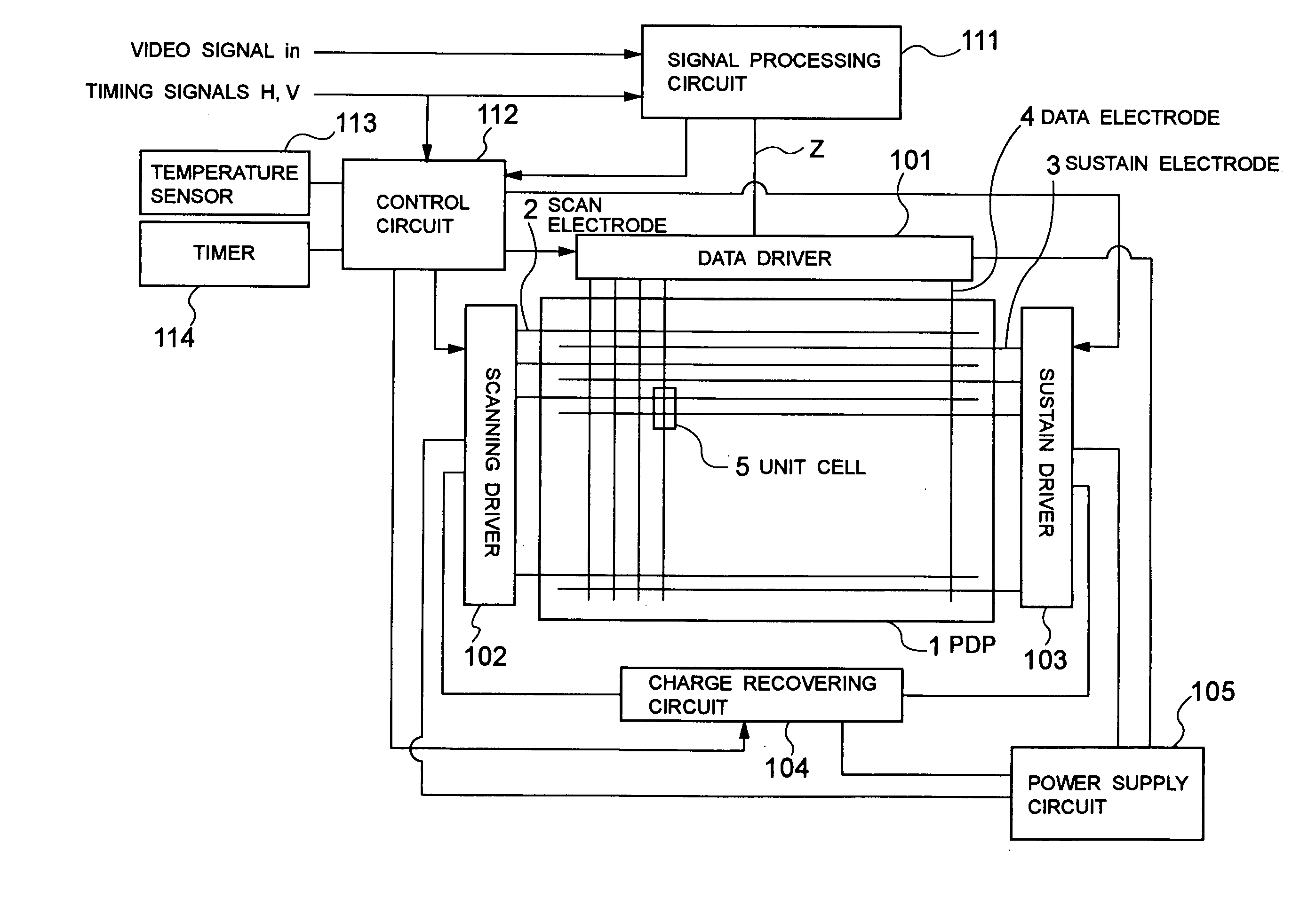
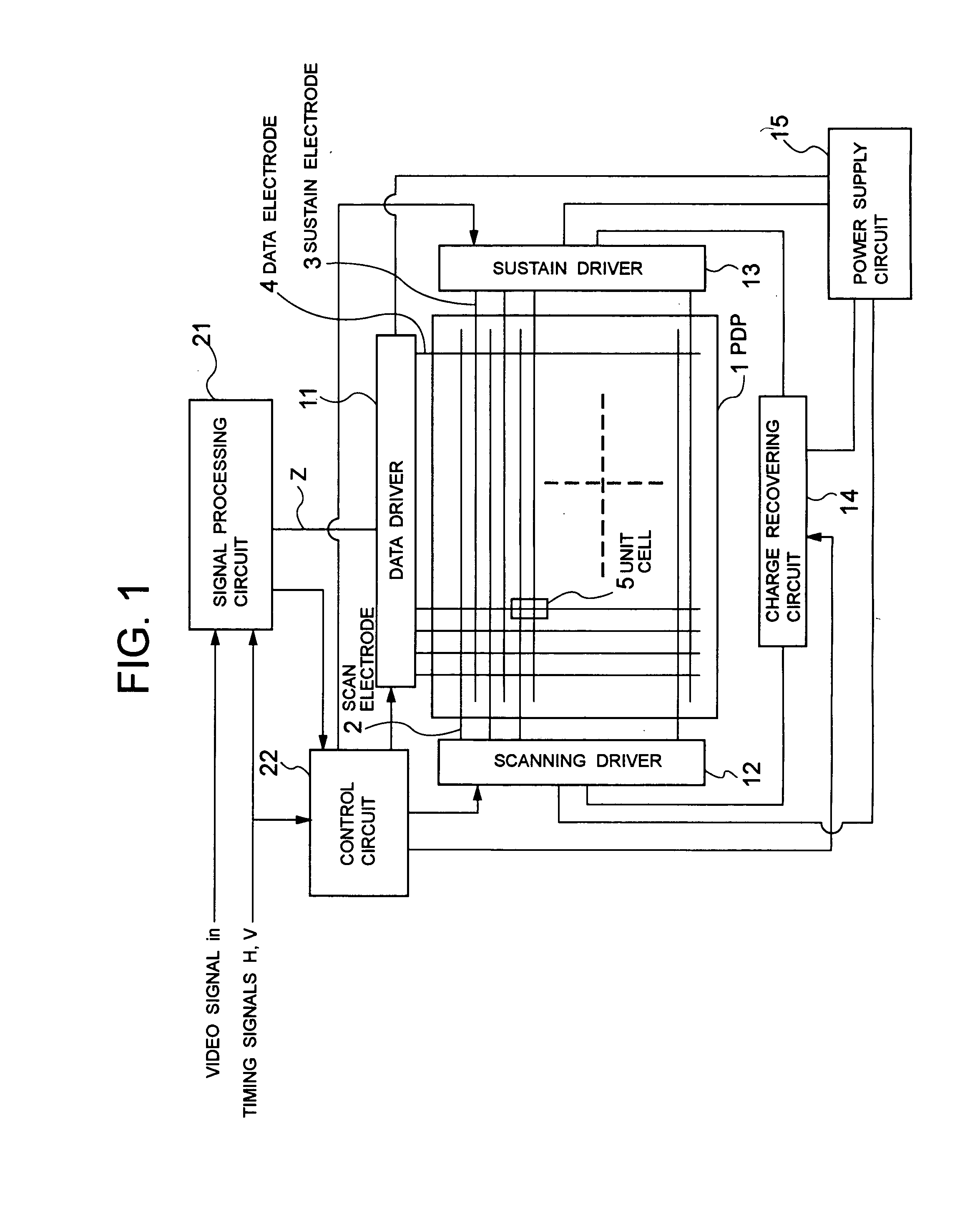
[0093]FIG. 10 is a block diagram showing an electric arrangement of a plasma display in this invention, wherein the common references are attached to the elements common to the elements in the FIG. 1 prior art.

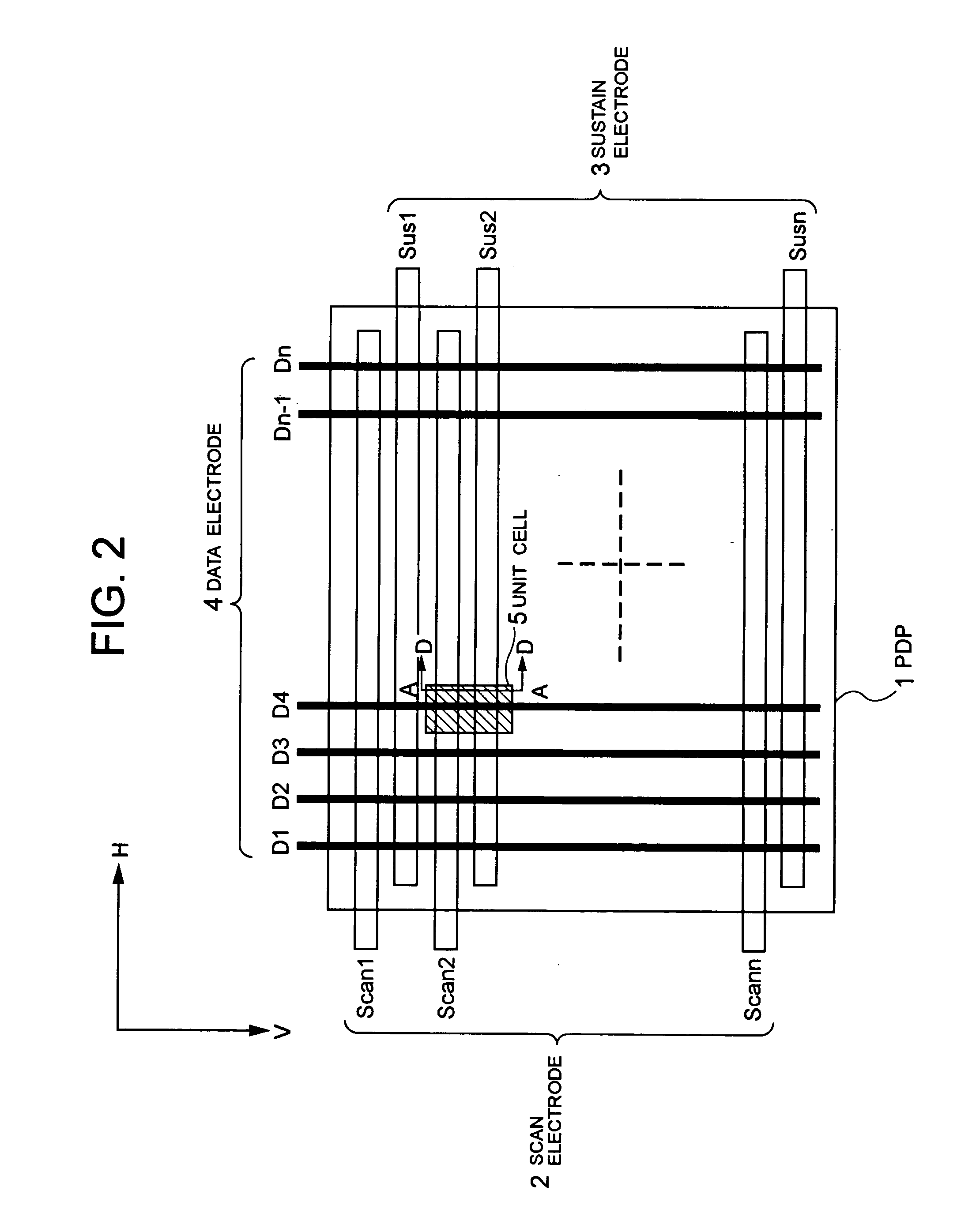
[0094] The plasma display in this embodiment is arranged with a display panel (PDP) 1, a data driver 101, a scanning driver 102, a sustain driver 103, a charge recovering circuit 104, a power supply circuit 105, a signal processing circuit 111, a control circuit 112, a temperature sensor 113 and a timer 114. The PDP 1 is structured similarly to the FIG. 2 prior art. The data driver 101 is to apply a data pulse and erase pulse corresponding to display data z, to the data electrode 4 of the PDP 1. The scanning driver 102 is to apply a scan pulse and erase pulse to the scan electrode 2 of the PDP 1. The sustain driver 103 is to apply a sustain pulse to the sustain electrode 3 of the PDP 1. The charge recovering circuit 104, having an inductance for recovering the charge on the ca...

second embodiment

[0126] As described above, in the second embodiment, because the sustain discharge emission intensity ratio is set smaller than 1, no image retention takes place. Furthermore, suppressed is the display non-uniformity due to the variation in discharge initiating threshold voltage.

[0127] Although the embodiments of the invention have been detailed so far, the detailed structure thereof is not limited to the same embodiment. Design modification, if made within a range not departing from the gist of the invention, is to be included in the invention.

[0128] For example, the charge recovering circuit 104 may be configured with inductances, to be controlled by the control circuit 112, in place of the inductances 61, 64, 71, 74, for example. Meanwhile, although in the first embodiment binary or ternary values were set for the load of display, the ambient environmental temperature, the time of use and so on in switching over the recovering time or the inductance value, much more values for s...


PUM


Abstract

A plasma display improved in variation of display brightness between unit cells. A control circuit sets, for every pulse, a charge-recovering time period for recovering a charge on a capacitance component of the plasma display panel and a clamp timing period for applying a predetermined sustain voltage to the sustain electrodes or the scan electrodes after the charge-recovering time period through clamp start timing, and sets a sustain-discharge emission intensity ratio, as a ratio of a maximal discharge intensity in the clamp timing period with reference to a discharge intensity in the clamp start timing to a maximum discharge intensity in the charge-recovering time period, at a value that a discharge in the clamp timing period is to spread up to an end of the unit cell. For example, the control circuit sets a sustain-discharge emission intensity ratio substantially at 0.5 or greater or 0.1 or smaller, thus eliminating the occurrence of image retention.

Description

BACKGROUND OF THE INVENTION [0001] 1. Field of the Invention [0002] This invention relates to a plasma display and a drive method for use on a plasma display, and more particularly to a plasma display and a drive method for use on a plasma display which are suitably used in improving the variations in brightness of display in a plasma display panel. [0003] 2. Description of the Related Art [0004] The plasma display, including a plasma display panel (hereinafter, referred also to as “PDP”) as its major part, has many features, e.g. sliminess and relative easiness to make a large-screen display, wide viewing angle, high response speed and so on. Consequently, it is a recent practice to make use of it as a flat panel display, in a wall-mounted TV and a communal display. [0005] The plasma displays are classified into a certain number of kinds depending upon the operation schemes thereof. The PDPs, manufactured presently on a commercial basis, adopts “Address Display Separate method (ADS...

Claims


Application Information

Patent Timeline
IPC IPC(8): G09G3/28G09G3/20G09G3/288G09G3/291G09G3/294G09G3/296G09G3/298
CPCG09G3/2965G09G2320/0233G09G2360/16G09G2320/041G09G2320/0257G09G3/294H01J11/22H01J11/34G09G3/296
Inventor MIZOBATA, EISHI
Owner PANASONIC CORP
Why Eureka
Try Eureka