

Linear array detector system and inspection method
a detector system and detector technology, applied in the field of imaging systems, can solve problems such as limited flexibility of arrays
- Summary
- Abstract
- Description
- Claims
- Application Information
AI Technical Summary
Benefits of technology
Problems solved by technology
Method used
Image

Examples
Embodiment Construction
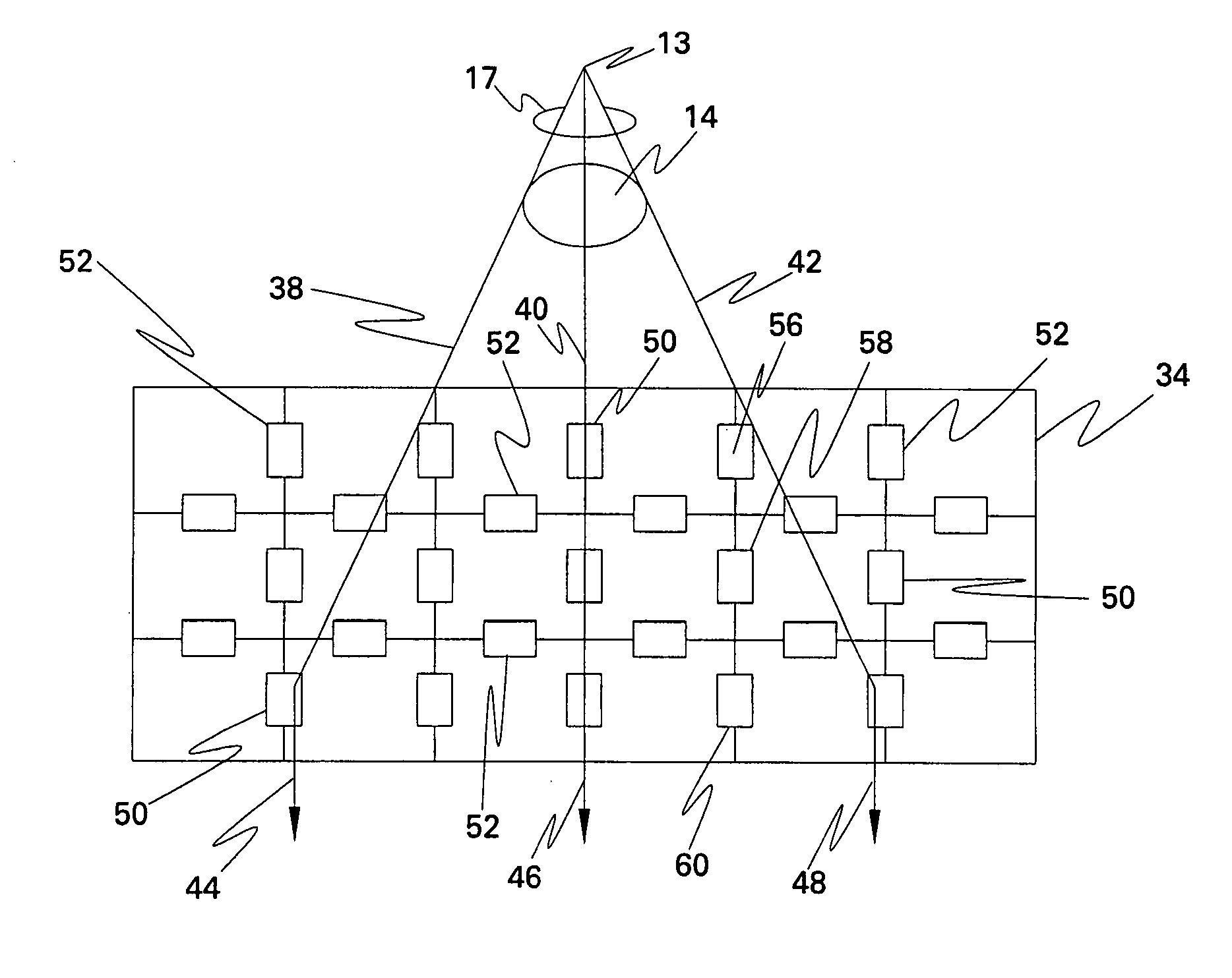
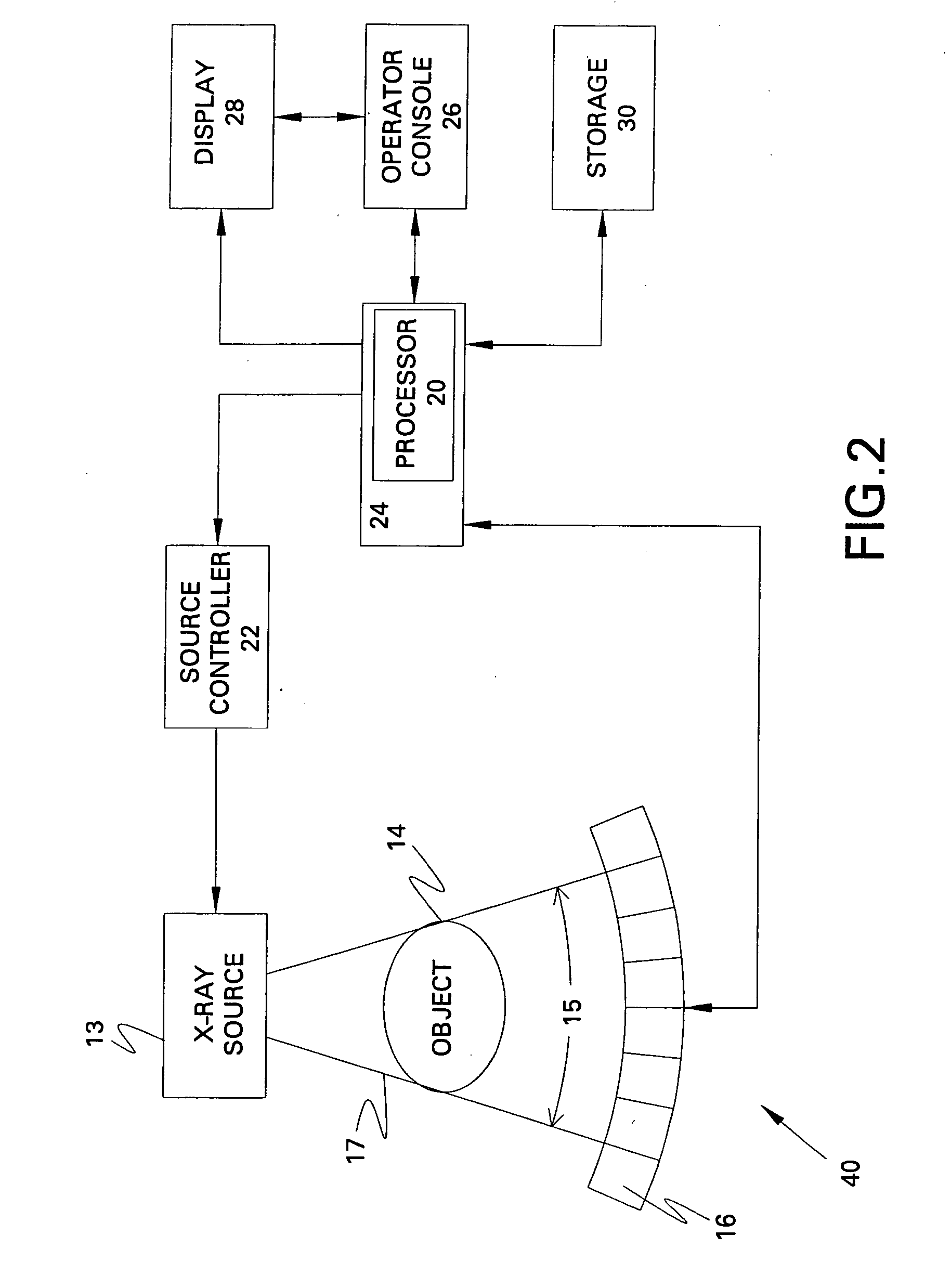
[0022]FIG. 2 is a block diagram of an embodiment of a system 10, which is an X-ray system designed both to acquire original image data and to process the image data for display and analysis in accordance with the present technique. Other imaging systems such as computed tomography system and digital radiography systems, which acquire image three dimensional data for a volume, also benefit from the present techniques. The following discussion of X-ray system 10 is merely an example of one such implementation and is not intended to be limiting in terms of modality.
[0023] As used herein, “adapted to”, “configured” and the like refer to devices in a system to allow the elements of the system to cooperate to provide a described effect; these terms also refer to operation capabilities of electrical or optical elements such as analog or digital computers or application specific devices (such as an application specific integrated circuit (ASIC)), amplifiers or the like that are programmed ...
PUM
 Abstract
Description
Claims
Application Information