
Semiconductor package

a technology of semiconductors and packages, applied in the direction of semiconductor devices, semiconductor/solid-state device details, electrical apparatus, etc., can solve the problems of low mounting reliability, insulating layer is susceptible to exfoliation, and the package thickness cannot be sufficiently reduced, so as to achieve high mounting reliability

Inactive Publication Date: 2006-04-06
SHARP KK
View PDF10 Cites 21 Cited by
  • Summary
  • Abstract
  • Description
  • Claims
  • Application Information

AI Technical Summary

Benefits of technology

[0010] The present invention has an object of providing a semiconductor package which is thin, multifunctional, and high in mounting reliability.

Problems solved by technology

However, burying passive components inevitably makes the insulating layer thicker than the passive components, making it impossible to sufficiently reduce the thickness of the package.
As a result, when the package is mounted on a motherboard (substrate), the insulating layer is susceptible to exfoliation, which indicates low mounting reliability.

Method used


Image

  • Semiconductor package
  • Semiconductor package
  • Semiconductor package

Examples


embodiment 1

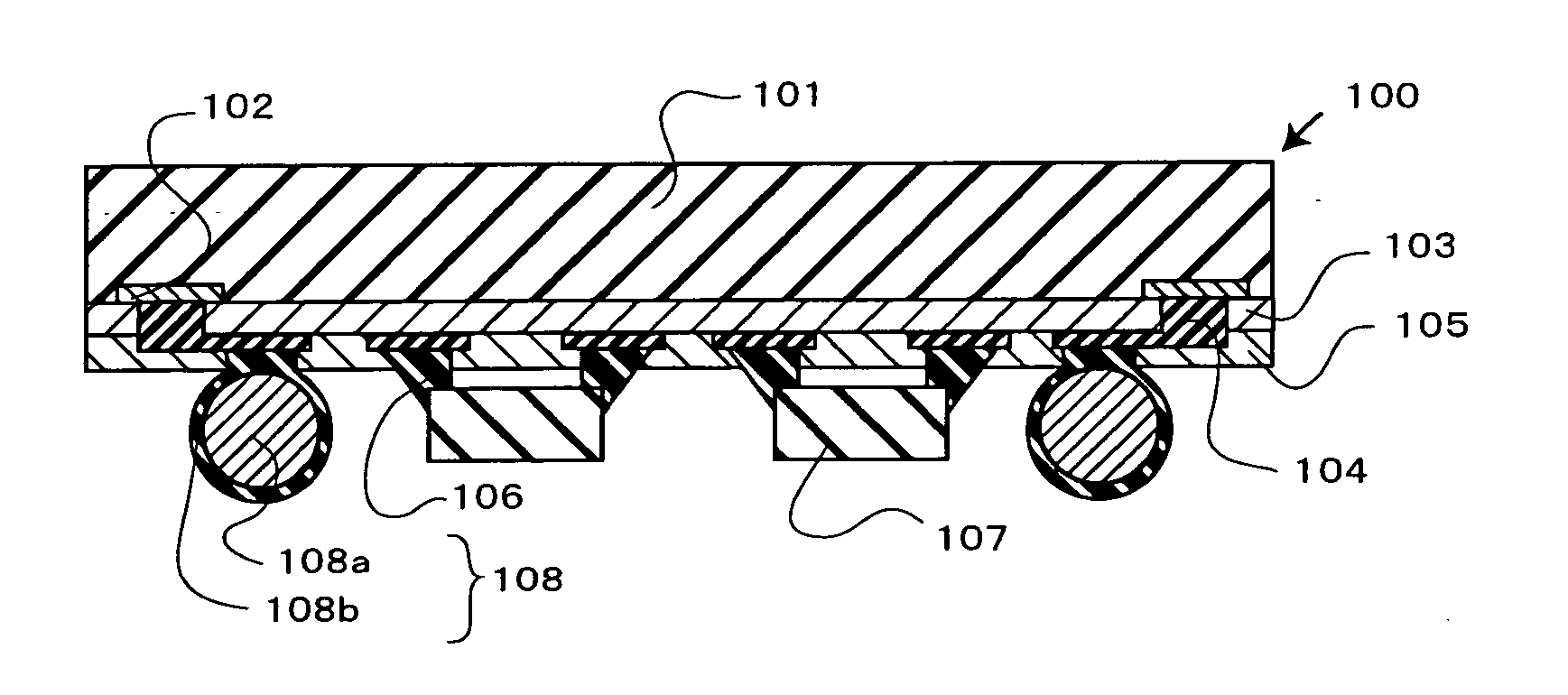
[0065] As shown in the schematic cross sectional view of FIG. 1, a semiconductor package 100 of the present embodiment includes an IC chip as a first electronic component 101; a first insulating film 103 which is in contact with one of the main surfaces of the IC chip; sheet-like internal wiring 104 which has a predetermined wiring pattern and is in contact with the first insulating film 103; a second insulating film 105 which is in contact with the internal wiring 104 and the first insulating film 103 and which faces the first insulating film 103 in such a manner as to sandwich the internal wiring 104; second electronic components 107 which are arranged outside the second insulating film 105; and spherical external output terminals 108 arranged outside the second insulating film 105 in the same manner as the second electronic components 107.

[0066] The IC chip and the external output terminals 108 are electrically continuous with each other by the connection between the external ou...

embodiment 2

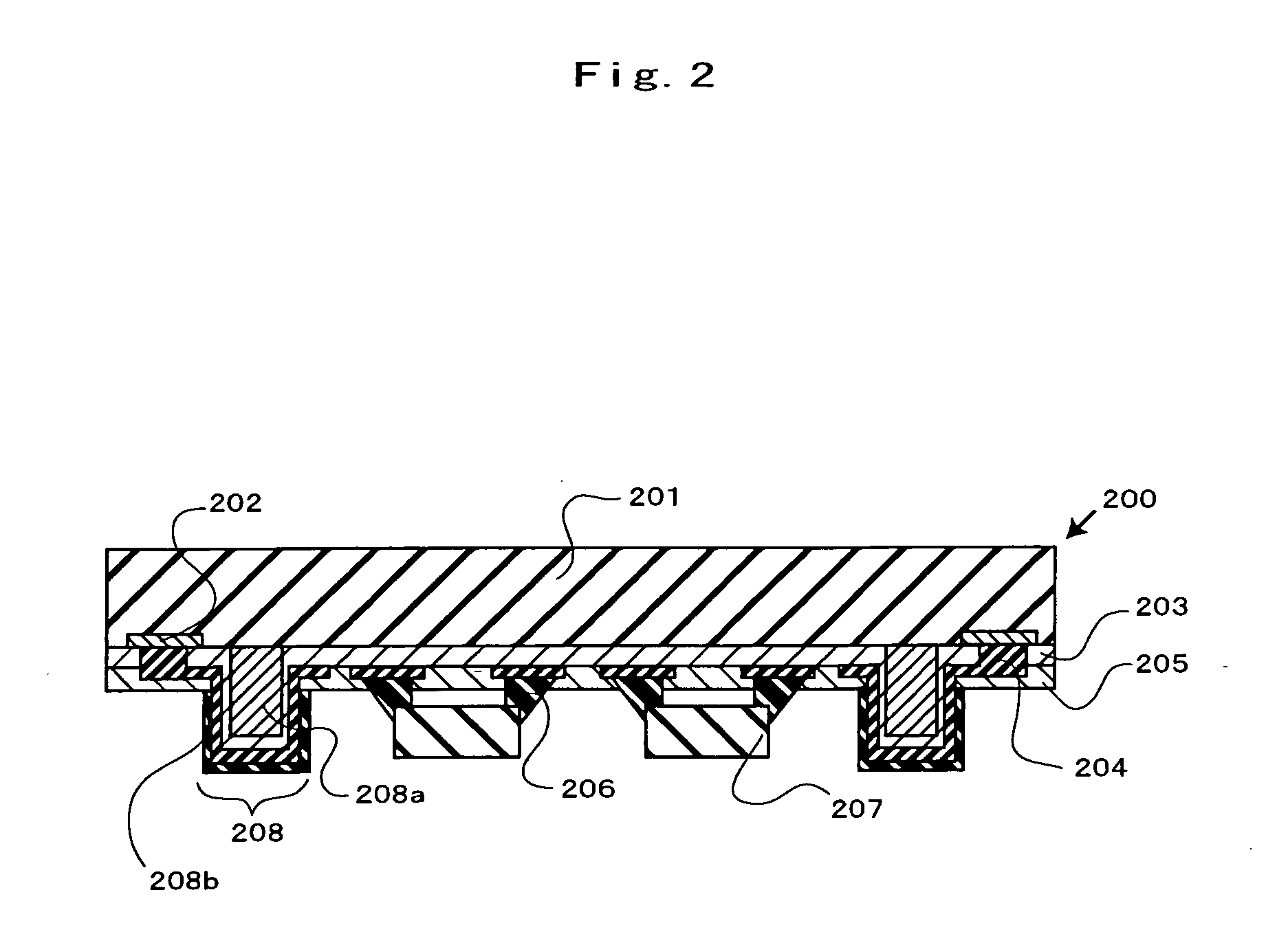
[0087] Embodiment 2 of the present invention will be described as follows with reference to accompanying drawings. Substantially the same components as those in embodiment 1 will not be described again.

[0088] As shown in the schematic cross sectional view of FIG. 2, a semiconductor package 200 of the present embodiment includes an IC chip as a first electronic component 201; cylindrical cores 208a which are formed outwardly on one of the main surfaces of the IC chip; a first insulating film 203 which is in contact with the one of the main surfaces of the IC chip and the cores 208a; sheet-like internal wiring 204 which is in contact with the first insulating film 203 and has a predetermined wiring pattern; a second insulating film 205, which will be described below; second electronic components 207 which are outside beyond the second insulating film 205; and solder 208b as surface layers to cover the extended parts of the internal wiring 204 that are outside beyond the second insula...


PUM


Abstract

A semiconductor package which is multifunctional, thin, and high in mounting reliability includes an insulating film; a first electronic component formed on one of the main surfaces of the insulating film; a second electronic component formed outwardly on the other of the main surfaces opposite to the one of the main surfaces; an external output terminal formed outwardly on the other of the main surfaces; and internal wiring formed in the insulating film so as to provide electrical continuity between the external output terminal and each of the first electronic component and the second electronic component. The insulating film is composed of a first insulating film and a second insulating film opposite to each other; the internal wiring is interposed between the first insulating film and the second insulating film, and the protruding end of the external output terminal is outside beyond the protruding end of the second electronic component.

Description

BACKGROUND OF THE INVENTION [0001] 1. Field of the Invention [0002] The present invention relates to a semiconductor package. [0003] 2. Description of the Prior Art [0004] In order to reduce electronic appliances such as mobile phones in size and weight, wafer-level chip scale packages (CSPs) have gotten attention as a semiconductor package to be mounted on an electronic appliance, because CSPs have the same size as semiconductor chips and can package a number of chips collectively while they are still in a wafer state. [0005] A wafer-level CSP includes a semiconductor chip; an insulating layer which is formed on the semiconductor chip and is provided with internal wiring electrically continuous with the semiconductor chip; and external output terminals which are formed on the internal wiring and are electrically continuous with the internal wiring. On the other hand, in order to make semiconductor packages more multifunctional, there is a technique of mounting, in addition to a sem...

Claims


Application Information

Patent Timeline
Patent Type & Authority Applications(United States)
IPC IPC(8): H01L23/34
CPCH01L23/49811H01L23/49816H01L23/49822H01L2924/1532H01L24/18H01L23/3114H01L2924/19041H01L2924/19104H01L24/13H01L2224/1403H01L2224/16145H01L2924/15321H01L2924/14H01L2224/05022H01L2224/05026H01L2224/05548H01L2224/0557H01L2224/05001H01L2224/05124H01L2224/05147H01L2224/05666H01L2224/05671H01L2224/05571H01L2224/16265H01L2224/14051H01L24/05H01L2224/02377H01L2924/00H01L2924/00014
Inventor SUMINOE, SHINJINAKANISHI, HIROYUKIKOMEDA, YOKO
Owner SHARP KK
Features
  • Generate Ideas
  • Intellectual Property
  • Life Sciences
  • Materials
  • Tech Scout
  • Unparalleled Data Quality
  • Higher Quality Content
  • 60% Fewer Hallucinations
Learn More