
Semiconductor Optical Device

Inactive Publication Date: 2007-12-13
STANLEY ELECTRIC CO LTD
View PDF10 Cites 29 Cited by
  • Summary
  • Abstract
  • Description
  • Claims
  • Application Information

AI Technical Summary

Benefits of technology

[0019]The presently disclosed subject matter has been devised in view of the above and other characteristics problems and features and includes a semiconductor optical device with high mounting reliability and the possibility of miniaturization. Another aspect of the disclosed subject matter includes a semiconductor light-emitting device that emits various light-emitting colors with excellent optical characteristics.

Problems solved by technology

As a result, a thermal conduction decrease of the lead frame electrode is caused by an increase of thermal resistance, and may result in a loss of radiation ability.
Thus, the increase in the number of lead frame electrodes results in a restrictive factor for designing a miniaturization of a semiconductor optical device size.
Thus, the decrease in area of respective other end portions may result in a decrease of mounting reliability because the semiconductor optical device may not be mounted with strength and confidence by the respective other end portions, and may result in a decrease of the light-emitting efficiency due to a rise of the operating temperature of an LED chip by weakening radiating efficiency of the LED chip's self-fever.
Furthermore, when a complex light-emitting color is emitted by a plurality of different light-emitting color LED chips, it is difficult to maintain a miniaturization of a semiconductor optical device size and to provide equal spacing intervals for the respective adjacent LED chips due to layout restrictions of the lead frame electrodes when positions of the one end portions must be moved in accordance with a layout of LED chips.
If each interval of the respective adjacent LED chips is forced to be equal, a semiconductor optical device may become large and may result in a decrease in the color rendering index because of long intervals between respective adjacent LED chips.

Method used


Image

  • Semiconductor Optical Device
  • Semiconductor Optical Device
  • Semiconductor Optical Device

Examples


Embodiment Construction

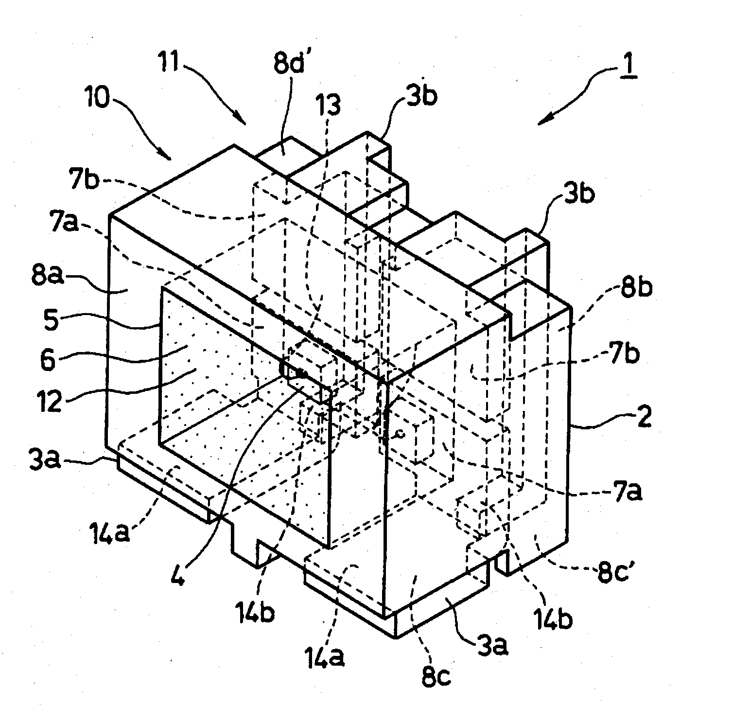
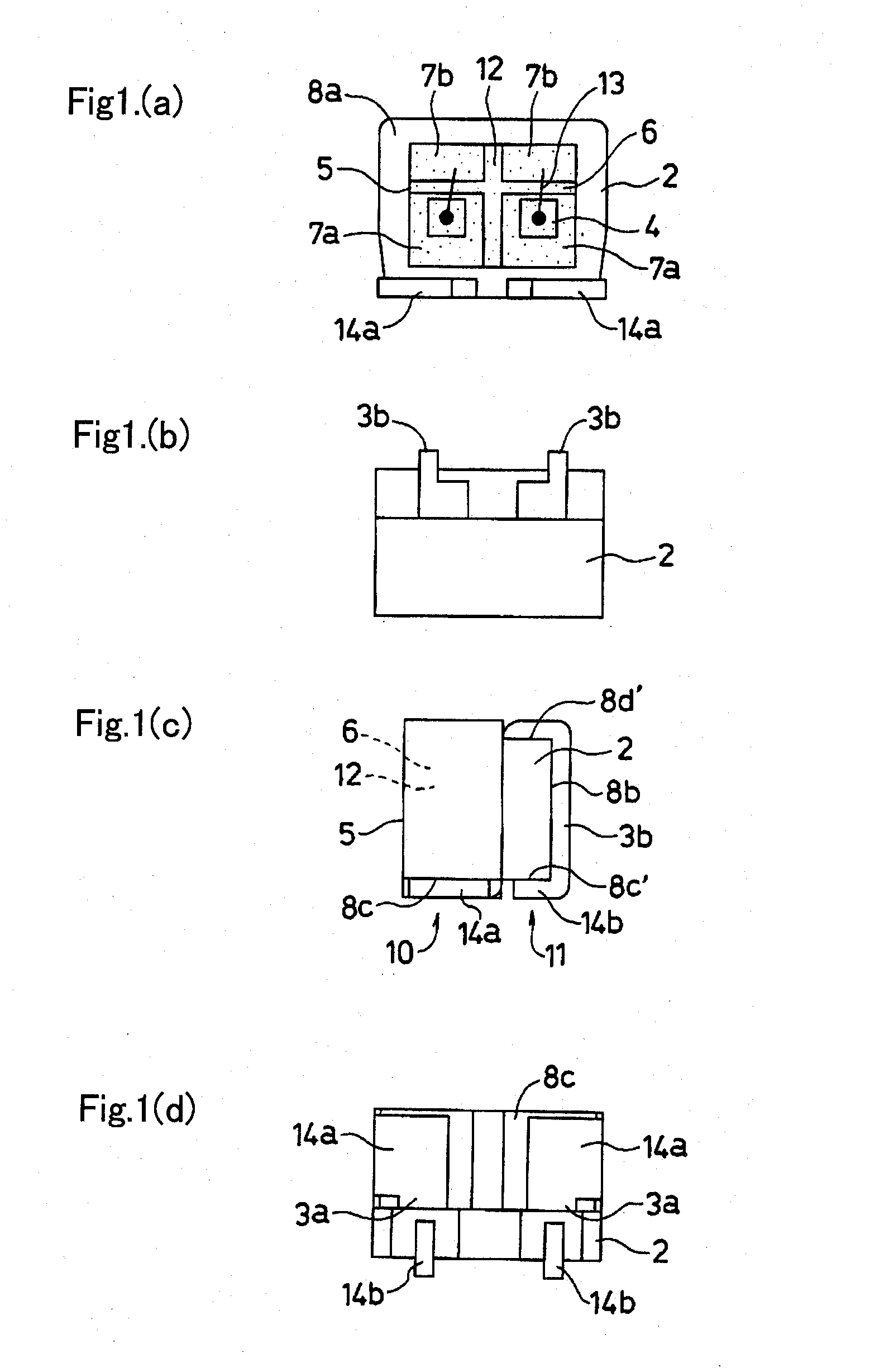
[0044]A first exemplary embodiment of the disclosed subject matter will now be described in detail with reference to FIGS. 1(a)-(d) and FIG. 2. FIGS. 1(a)-(d) show a front view, a top view, a side view, and a bottom view in turn for a semiconductor optical device in accordance with the first exemplary embodiment, and FIG. 2 shows the perspective view of the above device shown by FIGS. 1(a)-(d).

[0045]The semiconductor optical device 1 in accordance with the first exemplary embodiment can include: a casing 2 made from a resin; two pairs of lead frame electrodes 3a, 3b insert-formed in the resin casing; and semiconductor optical chips 4 having at least one of a light emitting / detecting function.

[0046]Actually, the casing 2 can consist of a resin formation, and at least one pair of lead frame electrodes 3a, 3b can be situated in or on the casing 2. The casing 2 defines the resin formation not including the pairs of lead frame electrodes 3a, 3b in the following described exemplary embodi...


PUM


Abstract

The disclosed subject matter includes a semiconductor optical device with a stable optical characteristic, an excellent radiant efficiency, and a high mounting reliability. A casing can be configured with a concaved-shaped cavity that includes an opening and a bottom portion. Each of one end portions of first / second lead frame electrodes 3a, 3b can be exposed on the bottom portion. The first one end portion can include an optical chip mounted thereon, and the second one end portion can be connected to another electrode of the optical chip via a bonding wire. The first lead frame electrode extends from an outside surface substantially perpendicular to the bottom portion and is bent in a direction towards the opening. The second lead frame electrode extends from an outside surface of the casing that is opposite to the outside surface from which the first electrode extends. Various physical configurations of the electrodes are disclosed.

Description

[0001]This application claims the priority benefit under 35 U.S.C. §119 of Japanese Patent Application No. 2006-139095 filed on May 18, 2006, which is hereby incorporated in its entirety by reference.BACKGROUND[0002]1. Field[0003]The presently disclosed subject matter relates to a semiconductor optical device including LEDs, laser diodes, photodiodes, etc. and more particularly to a surface mount semiconductor optical device, which emits / detects light in parallel with a mounting surface thereof (e.g., a side view type semiconductor device).[0004]2. Description of the Related Art[0005]A surface mount semiconductor optical device having a semiconductor optical chip mounted in a casing that is provided with lead frame electrodes insert-formed by a resin includes the following two types. One is a top view type, in which a light ray axis is perpendicular to a circuit board on which the chip is mounted. The other is a side view type, in which a light ray axis is parallel to the circuit bo...

Claims


Application Information

Patent Timeline
IPC IPC(8): H01L23/495H01L33/50H01L33/56H01L33/62H01L33/64
CPCH01L25/0753H01L31/0203H01L33/486H01L33/62H01L33/647H01L2224/48247H01L2224/48465H01L2924/00
Inventor HANYA, AKIHIKO
Owner STANLEY ELECTRIC CO LTD
Features
  • Generate Ideas
  • Intellectual Property
  • Life Sciences
  • Materials
  • Tech Scout
  • Unparalleled Data Quality
  • Higher Quality Content
  • 60% Fewer Hallucinations
Learn More