Barrier film and method for manufacturing same

Active Publication Date: 2016-07-14
LG CHEM LTD
View PDF6 Cites 0 Cited by
  • Summary
  • Abstract
  • Description
  • Claims
  • Application Information

AI Technical Summary

Benefits of technology

[0061]A barrier film according to the present application can be applied to organic or inorganic light-emitting devices, display devices, and photovoltaic devices and thereby

Problems solved by technology

Electric devices and metal wires that constitute the interior of devices such as organic or inorganic light-emitting device, display devices, and photovoltaic devices, when brought into contact with external chemical materials such as oxygen and moisture, tend to deteriorate or get oxidized, and become unable to perform their designated functions.
However, glass has the disadvantage that it is not only heavy but also brittle a

Method used


Image

  • Barrier film and method for manufacturing same
  • Barrier film and method for manufacturing same
  • Barrier film and method for manufacturing same

Examples


example 1

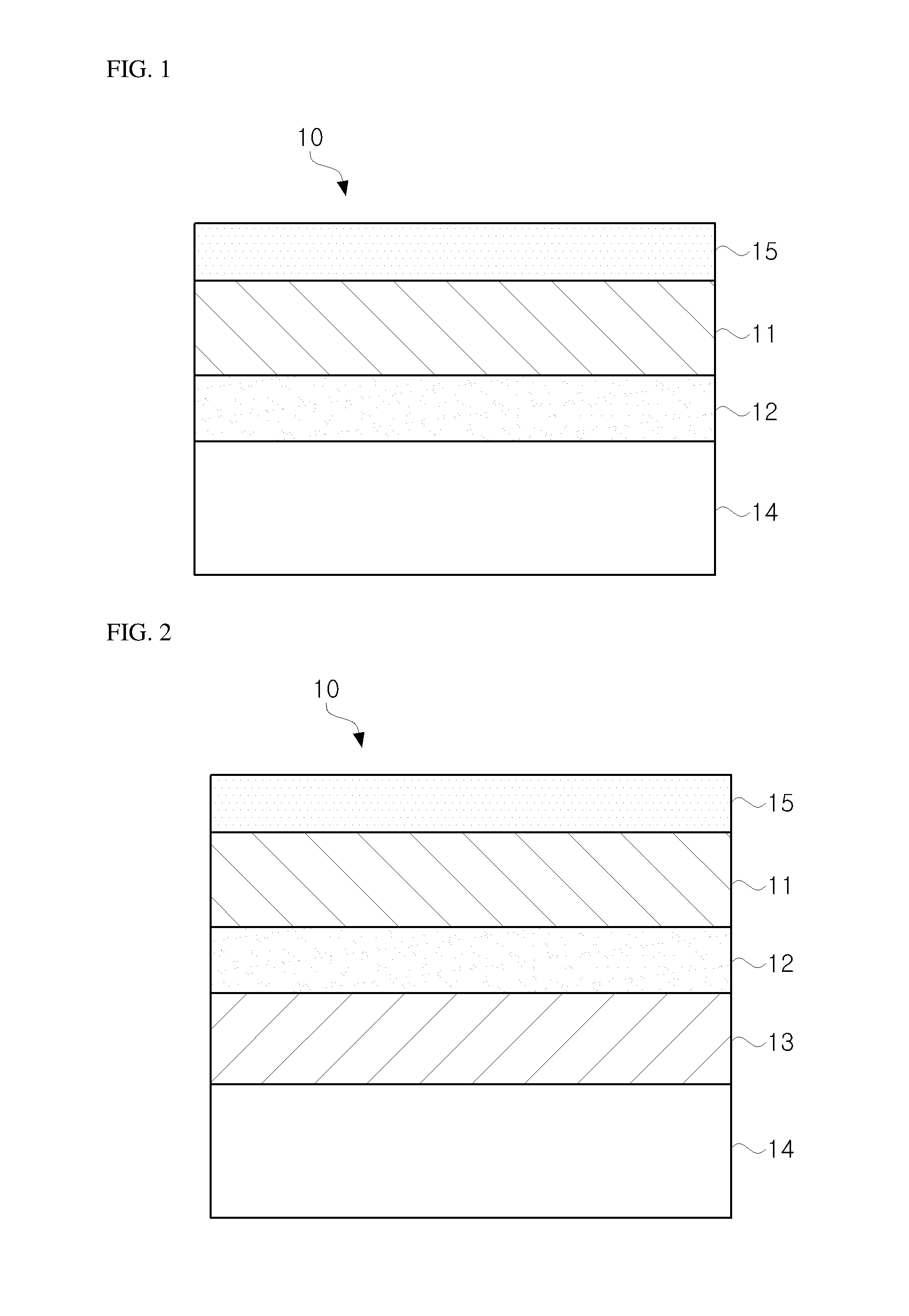
[0070]On a COP film (thickness 50 μm, refractive index 1.53) as a substrate layer, a coating solution comprising acrylic resin and metal oxide nanoparticles (TYT60, Toyoink Co.) was used to form a first dielectric layer having a refractive index of 1.60 to a thickness of 220 nm. On the coated film, zinc-tin oxide was laminated by sputtering as an inorganic layer having a thickness of about 19 nm and a refractive index of 2.0. On this laminated layer, by using the same coating solution, a second dielectric layer was formed to a thickness of 220 nm and, on this second dielectric layer, a resin layer having a refractive index of 1.52 and a thickness of 50 μm (LBPSA-LX150, LG Chemical Inc.) was laminated, to produce a barrier film.

[0071]EXAMPLE 2

[0072]A barrier film was prepared by the method described in Example 1 except that a first dielectric layer and a second dielectric layer were prepared to have a thickness of 90 nm.

example 3

[0075]On a COP film (thickness 50 μm, refractive index 1.53) as a substrate layer, a first dielectric layer having a refractive index of 1.65 was formed to a thickness of 220 nm by using a coating solution comprising acrylic resin and metal oxide nanoparticles (TYT65, Toyoink Co.). On the coated film, zinc-tin oxide was laminated by sputtering as an inorganic layer having a thickness of about 19 nm and a refractive index of 2.0. On this laminated layer, a second dielectric layer was formed to a thickness of 220 nm and having a refractive index of 1.48 by heat-curing a coating solution formulated with pentaerythritol triacrylate and methylethoxy silane at a ratio of 40:60, and on the second dielectric layer, a resin layer having a refractive index of 1.52 and a thickness of 50 μm (LBPSA-LX150, Lg Chemical) was laminated, to produce a barrier film.

example 4

[0076]A barrier film was prepared by the method described in Example 3 except that a first dielectric layer having a refractive index of 1.48 was formed by heat-curing a coating solution formulated with pentaerythritol triacrylate and methylethoxy silane at a ratio of 40:60, and a second dielectric layer having a refractive index of 1.65 was formed by using a coating solution comprising acrylic resin and metal oxide nanoparticles (TYT65, Toyoink Co.).


PUM

PropertyMeasurementUnit
Thicknessaaaaaaaaaa
Nanoscale particle sizeaaaaaaaaaa

Abstract

The present application relates to a barrier film and a method of preparing the same, and provides a barrier film that can be applied to devices such as organic or inorganic light-emitting devices, display devices, and photovoltaic devices and thereby effectively insulate the internal electric components from chemical materials such as moisture and oxygen while maintaining excellent optical characteristics at the same time.

Description

TECHNICAL FIELD[0001]The present application relates to a barrier film and a method for preparing the same.BACKGROUND ART[0002]Electric devices and metal wires that constitute the interior of devices such as organic or inorganic light-emitting device, display devices, and photovoltaic devices, when brought into contact with external chemical materials such as oxygen and moisture, tend to deteriorate or get oxidized, and become unable to perform their designated functions. Therefore, there is a need to protect the electric components from such chemical materials. To this end, the use of a glass plate as a substrate material or cover plate has been proposed as a means to insulate the chemical-sensitive internal devices. Glass plates have the advantages that they are adequate in terms of light transmittance, thermal expansion coefficient and chemical resistance. However, glass has the disadvantage that it is not only heavy but also brittle and fragile, requiring much caution in handlin...

Claims


Application Information

Patent Timeline
IPC IPC(8): B32B7/02B32B7/023
CPCB32B7/02B32B2457/00B32B2307/418B32B2307/204B32B27/08B32B27/16B32B27/325B32B27/36B32B27/365B32B27/38B32B27/40B32B27/42B32B2250/26B32B2255/10B32B2255/20B32B2255/24B32B2255/28B32B2264/10B32B2270/00B32B2307/40B32B2307/412B32B2307/546B32B2307/558B32B2307/718B32B2307/7244B32B2307/7246B32B2307/732B32B2457/12B32B2457/20B32B7/023
Inventor HWANG, JANG YEONKIM, DONG RYUL
Owner LG CHEM LTD
Why Eureka
Try Eureka