

Graphene sheet, transparent electrode and active layer including the same, and display, electronic device, optoelectronic device, battery, solar cell, and dye-sensitized solar cell including transparent electrode or active layer
a transparent electrode and active layer technology, applied in the field of graphene sheets, can solve the problems of reduced economic efficiency, increased cost, depletion of indium deposits of earth, etc., and achieve excellent physical, electrical, optical characteristics, excellent electrical and optical characteristics, excellent chemical, electrical and optical characteristics
- Summary
- Abstract
- Description
- Claims
- Application Information
AI Technical Summary
Benefits of technology
Problems solved by technology
Method used
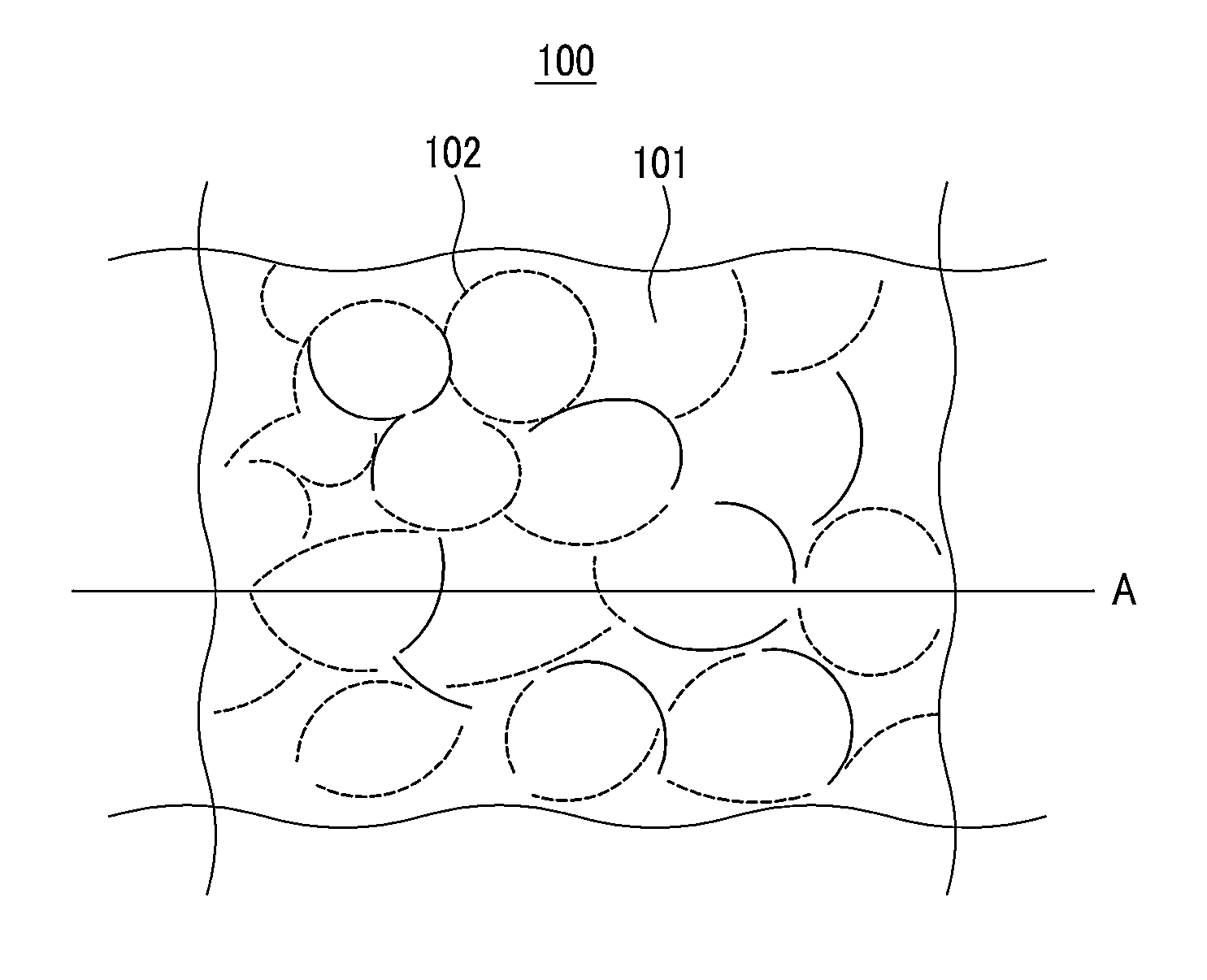
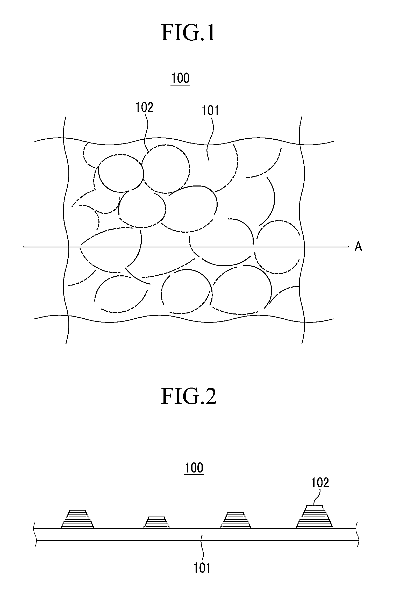
Image

Examples
example
Manufacturing the Graphene
Example 1
Formation of the Graphene on the SiO2 / Si Substrate
[0309]In the present example, a liquid carbon source material was used to form the graphene on the SiO2 / Si substrate. The thickness of the SiO2 layer was 300 nm, and SiO2 was deposited on the Si substrate by using the thermal growth method.
[0310]After the surface of the SiO2 / Si substrate was cleaned, for deposition of the metal thin film, the 100 nm-thick nickel thin film was deposited on the substrate by using the electron beam evaporator. The temperature of the substrate was maintained at 400° C. during the deposition.
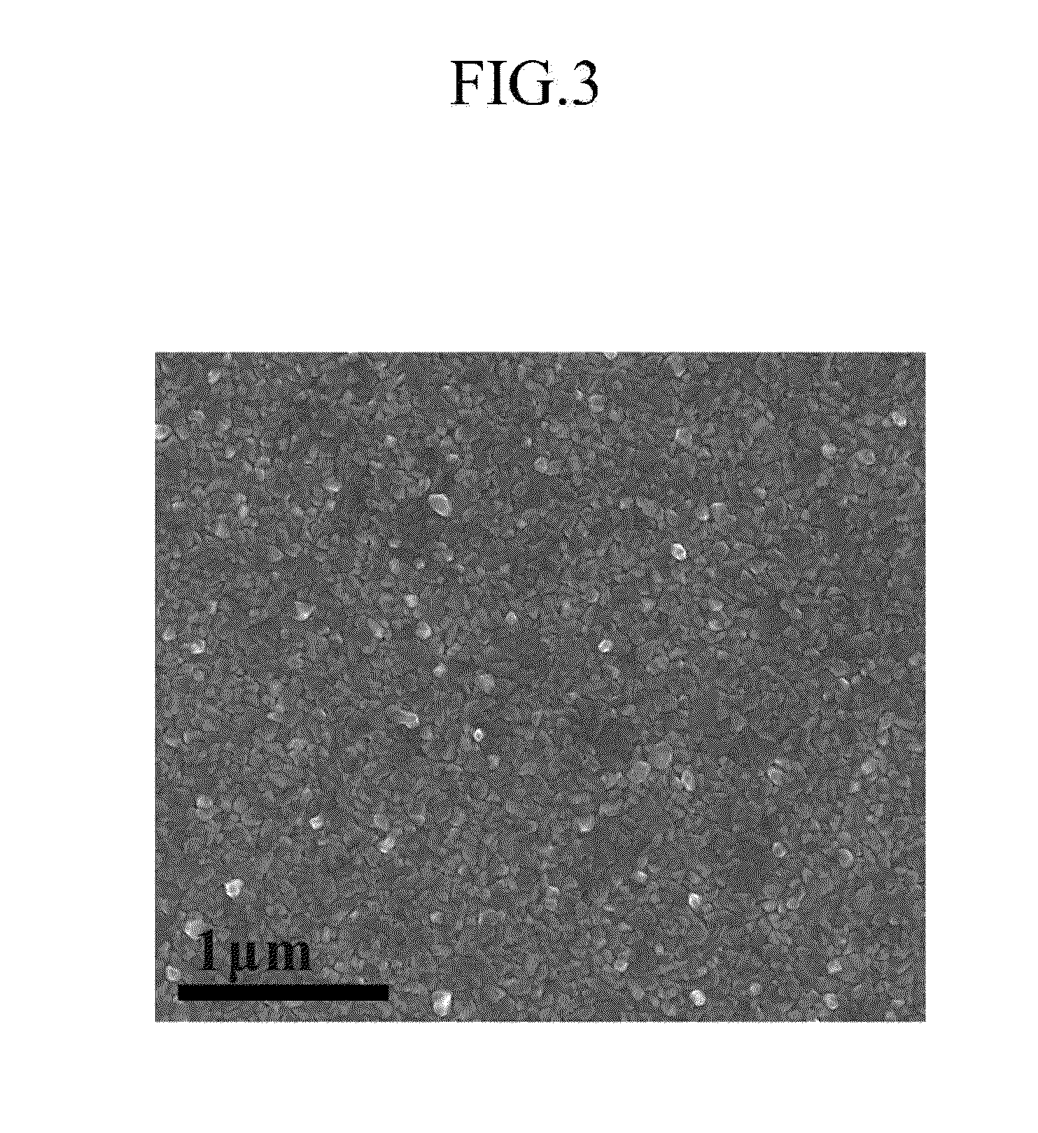
[0311]FIG. 3 is a SEM image of the nickel thin film deposited in Example 1.
[0312]It can be identified that the polycrystalline nickel thin film was formed, and it can be seen that the grain size was about 50 nm to 150 nm (average 100 nm).
[0313]The heat treatment process was performed in order to improve the orientation and to increase the average grain size in the nickel thin film. T...
example 2
[0322]A graphene sheet was manufactured according to the same method as Example 1, except that the heat treatment temperature was set to 160° C. after putting the carbon source material onto the nickel thin film in Example 1.
[0323]FIG. 7 is a SEM image of the graphene sheet according to Example 2, and FIG. 8 is an optical microscope image of the graphene sheet according to Example 2.
[0324]As shown in FIG. 7, it can be identified that the graphene of Example 2 had very large grains with the size ranging from several micrometers to several tens of micrometers. The SEM images show a clear difference in brightness contrast depending on the thickness of the graphene. The lightest image corresponds to the monolayer graphene C, the light image corresponds to the bilayer graphene B, and the darkest image corresponds to the multi-layered graphene A. The multi-layered graphene corresponds to the ridge.
[0325]From FIG. 7 it can be seen that the ridge portion is continuously or discontinuously s...
example 3
[0329]The graphene was manufactured according to the same method as Example 1, except that heat treatment temperature and the heating maintenance time were set to 60° C. and 10 minutes, respectively, after putting the carbon source material onto the nickel thin film in Example 1.
PUM
| Property | Measurement | Unit |
|---|---|---|
| size | aaaaa | aaaaa |
| size | aaaaa | aaaaa |
| size | aaaaa | aaaaa |
Abstract
Description
Claims
Application Information