Grapheme based electronically controlled terahertz attenuation piece, preparation method and utilization method
An attenuator and terahertz technology, applied in the field of terahertz band devices, can solve problems such as poor stability, non-tunable, narrow working frequency band, etc.
- Summary
- Abstract
- Description
- Claims
- Application Information
AI Technical Summary
Problems solved by technology
Method used
Image
Examples
Embodiment 1
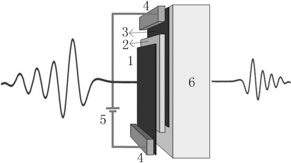
[0082] figure 1 Shown is an electronically controlled terahertz attenuator composed of two graphene layers, viewed from the side. The attenuation sheet includes a base 6, a three-layer structure is laid layer by layer above the base 6, including two graphene layers 1 and 3, and a dielectric layer 2 that completely separates the adjacent two graphene layers 1 and 3, graphite An electrode 4 is connected between the graphene layer 1 and the graphene layer 3 and a voltage 5 is applied.
Embodiment 2
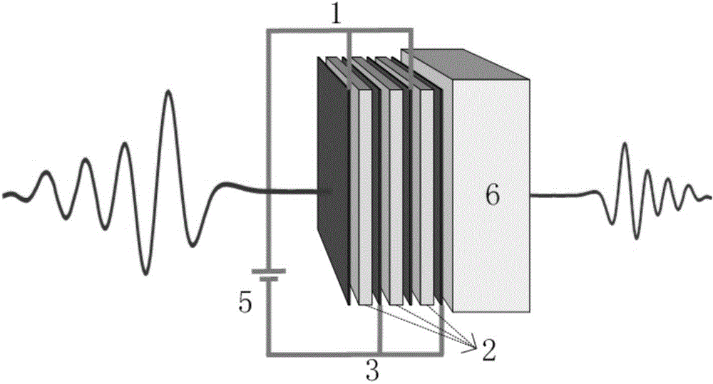
[0084] figure 2 Shown is an attenuation sheet made of 4 graphene layers, including a substrate 6, and a 7-layer structure is laid layer by layer on the substrate 6, including 4 graphene layers and between every two adjacent graphene layers. Between the medium layer 2. From left to right in the figure, the first and third graphene layers are respectively connected to one electrode, and the second and fourth graphene layers are respectively connected to another electrode. The voltage on these two electrodes is 5, an odd number Layers and even-numbered graphene layers each have the same potential, and a voltage of 5 can be applied to adjust the conductivity of each graphene layer. exist figure 2 In , the electrodes are not shown. In practical applications, the connection between conductive wires and graphene should be realized by making electrodes.
[0085] In actual design, the number of graphene layers is not limited to 2 layers and 4 layers, but changes according to the a...
Embodiment 3
[0087] In this embodiment, we select the following devices to prepare attenuation sheets comprising different graphene layers:
[0088] Graphene sample (fixed) parameters: area 1cm 2 , carrier scattering probability 100cm -1 , Fermi velocity v F =1.1×10 6 m / s, test temperature: 300K, preparation method: CVD.
[0089] (non-fixed) parameters of graphene: number of layers: 2-6, voltage: 0-80V.
[0090] Dielectric layer: SiO 2 , thickness: 50nm; method: magnetron sputtering, refractive index: 1.5.
[0091] Substrate: Quartz, thickness 500 μm, refractive index 1.5.
[0092] Electrodes: copper, magnetron sputtering.
[0093] The frequency of the incident terahertz wave is 1 THz. The Fermi energy level of graphene is 0eV and -0.315eV, and the corresponding voltage is adjusted from 0V to 80V, which is the upper and lower limits of the change of the Fermi energy level of graphene.
[0094] get Figure 6 The variation range of the terahertz wave extinction degree of the graphene...
PUM
| Property | Measurement | Unit |
|---|---|---|
| thickness | aaaaa | aaaaa |
| thickness | aaaaa | aaaaa |
| thickness | aaaaa | aaaaa |
Abstract
Description
Claims
Application Information


