Diamond cone and its making process

A diamond cone and diamond technology, applied in the field of diamond cone tip materials and their production, can solve the problems of inability to obtain electrical information and morphology information, diamond tip wear resistance, and low mechanical application potential, etc., and achieve excellent electrical and mechanical applications. The effects of mechanical properties, controllable hardness and stable electrical conductivity

Inactive Publication Date: 2006-05-17
INST OF PHYSICS - CHINESE ACAD OF SCI
View PDF0 Cites 17 Cited by
  • Summary
  • Abstract
  • Description
  • Claims
  • Application Information

AI Technical Summary

Problems solved by technology

[0007] The object of the present invention is to: not only overcome the defects that the existing diamond tip manufactured by the diamond film attachment method is not resistant to wear, easy to fall off and easy to lose electrical properties, but also overcome the existing bulk diamond tip that has too high a length-to-diameter ratio. Small, large radius of curvature, but can not obtain complete electrical information and morphology

Method used


Image

  • Diamond cone and its making process
  • Diamond cone and its making process
  • Diamond cone and its making process

Examples


Embodiment 1

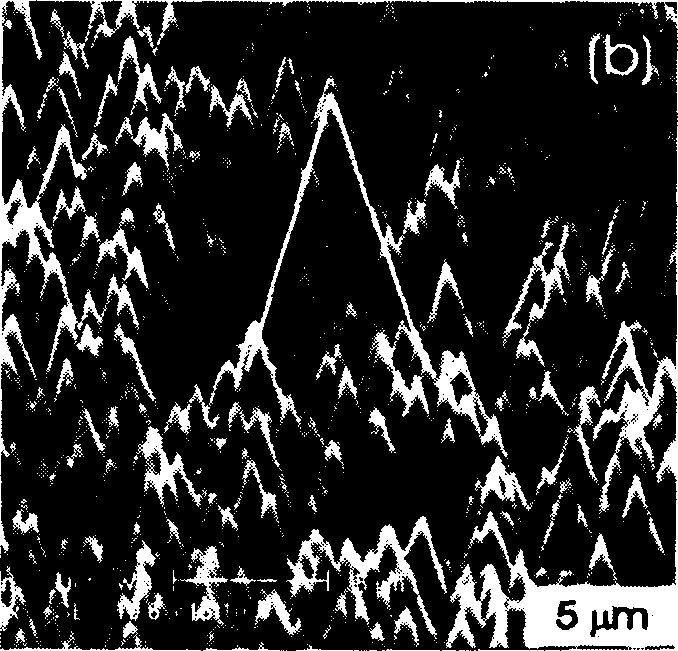
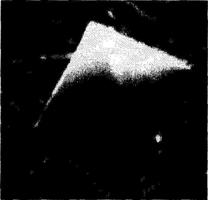
[0047] The specific structure of the diamond cone tip of the present embodiment refers to the attached Figure 5 (a); The diamond tip has an aspect ratio of 5, a tip curvature radius of 100 nanometers, and a bottom diameter of 4 microns.

[0048] refer to Figure 4 a-4f, the method of the present invention is described in detail according to its flow chart.

[0049] 1. On the surface of the monocrystalline silicon substrate 2, use a coating machine to spin coat a layer of PMMA photoresist with a thickness of about 200-300 nanometers as the protective layer 1 with a concentration of 5%. The coating conditions are: rotating speed 4000 RPM, spin coating time is 1 minute;

[0050] 2. Put the silicon substrate 2 that has been coated with the protective layer 1 into the cavity of the focused ion beam system, and use the ion beam to etch a conical hole 3 with a diameter of 4 microns and a depth of 20 microns on the silicon wafer. That is, the silicon template is obtained; the comm...

Embodiment 2

[0055] The specific structure of the planar diamond tip of the present embodiment can be found in Figure 5 (b): The diamond cone tip has an aspect ratio of 6.75, a tip curvature radius of about 100 nanometers, and a bottom diameter of 2 microns.

[0056] refer to Figure 4 a-4f, the difference between this embodiment and embodiment 1 is that the gas-assisted ion beam etching technique is used to etch a conical hole 3 with a diameter of 2 microns and a depth of 13.5 microns, to obtain a silicon template. The etching process parameters: ion source voltage (30KV), ion beam current (1nA), beam spot spacing (50% of the beam spot diameter), and beam current residence time (1 microsecond) were not changed. All the other conditions are with embodiment 1. The diamond tip ( Figure 5 (b)) The upper part is conical, and there is an obvious step in the middle part, which is beneficial to the improvement of the overall strength. When the diameter of the etched hole is greater than 1 m...

Embodiment 3

[0058] The specific structure of the diamond cone tip of the present embodiment refers to the attached Figure 5 (c), the diamond cone tip has an aspect ratio of 7.7, a tip curvature radius of 30 nanometers, and a bottom diameter of 1 micron.

[0059] refer to Figure 4 a-4f, the difference between the method of the diamond tip made in the present embodiment and the embodiment 1 is that the gas-assisted ion beam is used in the present embodiment to etch a conical hole 3 with a diameter of 1 micron and a depth of 7.7 microns, i.e. Obtain a silicon template. Etching process parameters: ion source voltage (30KV), ion beam current (3nA), beam spot spacing (150% of beam spot diameter), and beam current residence time (0.2 microseconds) have all been changed. The diamond tip ( Figure 5 (c)) In addition to having a large base, the top is tapered and conical. When the diameter of the etched hole is greater than 1 micron, its relative shape does not change with the diameter of the ...


PUM


Abstract

The present invention relates to one kind of diamond cone and its making process, and the diamond cone has length/diameter ratio of 2-8, tip curvature radius smaller than 50 nm, and bottom diameter from 100 nm to decades of microns. The making process includes the following steps: coating one protecting layer onto silicon substrate; etching with focused ion beam to form silicon template with conic holes for making the diamond cones; eliminating the protecting layer with etching agent; and growing continuous diamond film in traditional method to obtain the diamond cones. The diamond cone has high wear resistance, high hardness and controllable shape, and is ideal structure for field emitting device, scanning probe system, nanometer impression and miniature tool. Compared with traditional diamond cone making process, the process of the present invention is simple, efficient and suitable for mass production.

Description

technical field [0001] The present invention relates to a diamond tip material and a manufacturing method thereof, in particular to a diamond tip material which not only has a high aspect ratio and a small tip curvature radius, but also has a controllable aspect ratio and a controllable shape. Devices, scanning probe systems, nano-imprinting and micro-tools all have diamond cone tips and manufacturing methods with great application prospects. Background technique [0002] There are roughly three existing techniques for making diamond tips: growing diamond thin films on the tips; ion etching of diamond films; template method to make pyramid-shaped diamond tips. Now three kinds of existing techniques for making diamond tips are specifically described as follows: [0003] 1. Diamond tips made by growing diamond films on spikes: see Reference 1, "The fabrication of diamond tips by the microwave plasma chemical vapor deposition technique" (fabrication of diamond tips by the micr...

Claims


Application Information

Patent Timeline
IPC IPC(8): C23C16/27C23C16/458C23C16/50C23C16/513C23G1/00G03F7/00
Inventor 王宗利顾长志李俊杰
Owner INST OF PHYSICS - CHINESE ACAD OF SCI
Why Eureka
Try Eureka