Microlens substrate, a method for manufacturing the microlens substrate, a liquid crystal panel, and a projection type display apparatus

a technology of liquid crystal panel and microlens substrate, which is applied in the direction of identification means, instruments, projectors, etc., can solve the problems of deterioration of the product quality of the manufactured opposed substrate for affecting the manufacturing cost of the liquid crystal panel, and taking a considerable long time to manufacture the microlens substrate. achieve excellent optical characteristics and durability

Inactive Publication Date: 2007-03-01
138 EAST LCD ADVANCEMENTS LTD
View PDF2 Cites 6 Cited by
  • Summary
  • Abstract
  • Description
  • Claims
  • Application Information

AI Technical Summary

Benefits of technology

[0014] Accordingly, it is an object of the invention to provide a microlens substrate for an opposed substrate which has excellent optical characteristics and durability and can be suitably used in a liquid crystal panel.

Problems solved by technology

However, the method mentioned above requires many manufacturing steps and thus it takes a considerably long time for manufacturing a microlens substrate.
Therefore, use of the method gives a large affect to the manufacturing cost of a liquid crystal panel.
Further, since a large amount of grinding or polishing particles are generated in the grinding and polishing steps, it is necessary to wash the substrate during and after the grinding and polishing steps.
Since such washing is carried out using a large quantity of water, it is not desirable from the viewpoints of natural resource saving and environmental concerns.
In addition, there is a case that the photocuring resin material is deteriorated through the washing step, which may result in the case where the product quality of the manufactured opposed substrate for a liquid crystal panel is deteriorated.
Further, even in the case where such washing is carried out, there is a possibility that grinding or polishing particles still remain on the manufactured microlens substrate (that is, on the opposed substrate for a liquid crystal panel), so that it is difficult to raise the reliability of the manufactured microlens substrate to a sufficiently high level.
However, this method is not preferable in view of the optical characteristics of the microlens substrate because the thickness of the microlens substrate becomes a considerable thickness.
Further, use of such a microlens substrate having the considerable thickness leads to an increased size of a projection type display apparatus.
However, this method involves problems such as follows.
Namely, in general, photocuring resins have poor heat resistance, and therefore there is a case that the constituent material (photocuring resin material) of the microlens substrate is deteriorated due to heat applied when a black matrix and a common electrode are formed on the photocuring resin material constituting the microlens substrate, in particular when they are formed by a chemical vapor deposition method.
This means that if such a photocuring resin material is used as a constituent material of a liquid crystal panel, there is a possibility that any deformation occurs therein.
When such deformation occurs, Color Heterogeneity (uneven color distribution) occurs in an image to be displayed by the liquid crystal panel, which results in a lowered image quality of an image to be displayed.

Method used


Image

  • Microlens substrate, a method for manufacturing the microlens substrate, a liquid crystal panel, and a projection type display apparatus
  • Microlens substrate, a method for manufacturing the microlens substrate, a liquid crystal panel, and a projection type display apparatus
  • Microlens substrate, a method for manufacturing the microlens substrate, a liquid crystal panel, and a projection type display apparatus

Examples


example

Example 1

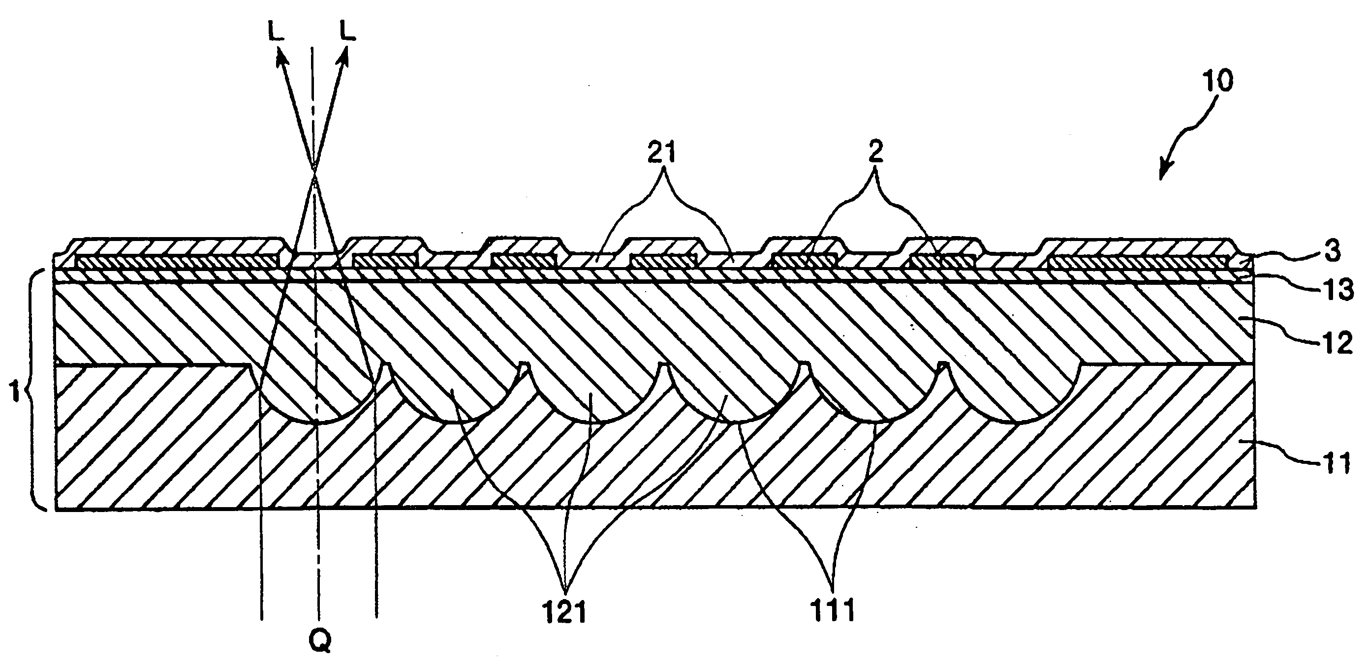
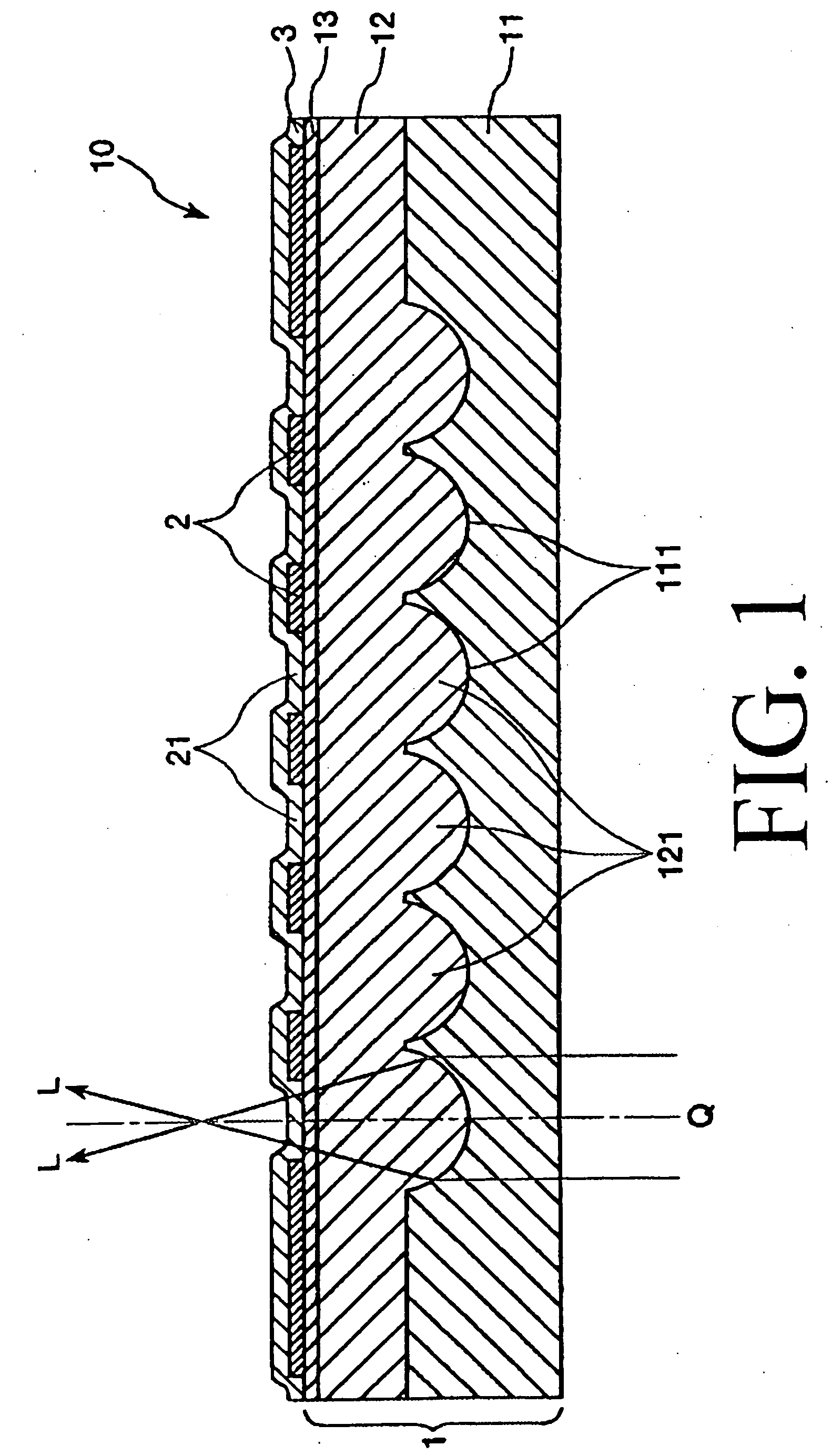
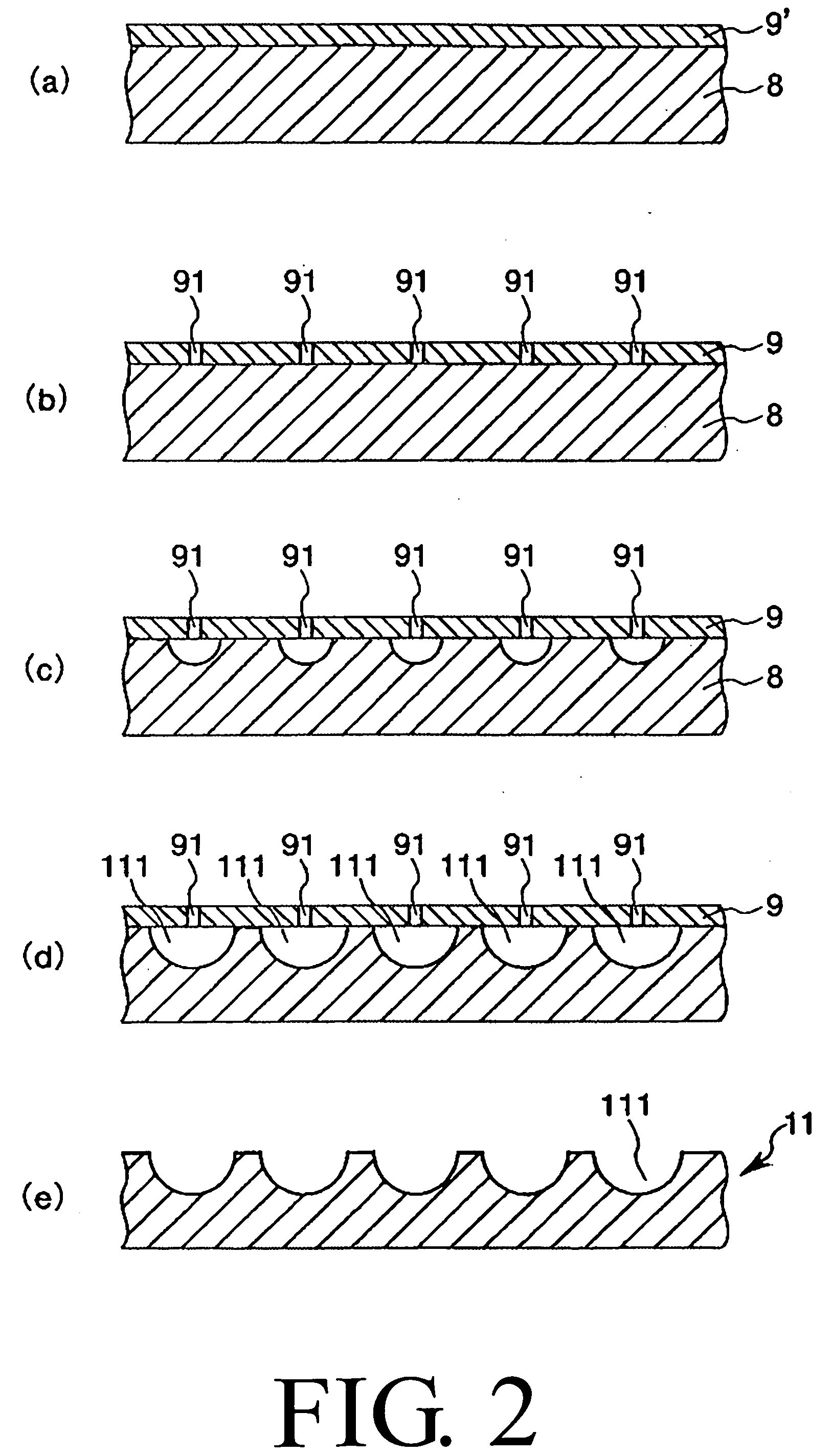
[0202] A substrate with concave portions provided with a plurality of concave portions was manufactured, and then a microlens substrate was manufactured using the substrate with concave portions in the following manner.

[0203]

[0204] First, a quartz glass substrate (which has an index of refraction of 1.46) having a thickness of 2 mm was prepared as a glass substrate.

[0205] The quartz glass substrate was soaked in a cleaning liquid (that is, a mixture of 80 vol % sulfuric acid solution and 20 vol % hydrogen peroxide solution) heated to 85° C. to be washed, thereby cleaning its surface.

[0206] Next, Cr films each having a thickness of 0.03 μm were formed on the quartz glass substrate by means of a spattering method. Namely, a film for forming a mask and a rear face protective film formed of the Cr films were formed on the both major surfaces of the quartz glass substrate.

[0207] Next, a laser machining was carried out with respect to the film for forming a mask, whereby a l...

example 2

[0232] Microlens substrates (total 100 pieces) were manufactured in the same manner as in the Example 1 described above except that as a composition for forming the convex lens substrate, a composition mainly constituted of an organic-inorganic composite material (epoxy resin-silica composite material) was used. In this Example 2, an index of refraction of the constituent material of the convex lens substrate was 1.57. Further, an amount of silica contained in the epoxy resin-silica composite material was 35 wt %, and an amount of the epoxy resin contained in the epoxy resin-silica composite material was 65 wt %.

examples 3 and 4

[0233] In each of the Examples 3 and 4, microlens substrates (total 100 pieces) were manufactured in the same manner as in the Example 1 described above except that initial hole formation condition and etching condition against the a mask formation film when manufacturing the substrate with concave portions as well as composition of the coating layer formation composition and the amount of the supply of the composition were changed so that the composition, properties and thickness of the convex lens substrate were changed.


PUM

PropertyMeasurementUnit
viscosityaaaaaaaaaa
thicknessaaaaaaaaaa
wavelengthaaaaaaaaaa

Abstract

A microlens substrate for an opposed substrate for use in a liquid crystal panel is provided. The microlens substrate includes: a substrate with concave portions having a plurality of concave portions; a convex lens substrate having convex lenses, each of the convex lenses having a shape corresponding to each of the concave portions, and the convex lens substrate being provided with respect to the substrate with concave portions so that the convex lenses are opposed to the corresponding concave portions, respectively; and a coating layer provided on the surface of the convex lens substrate which does not face the substrate with concave portions, the coating layer being mainly constituted of a product material produced by a reaction of a polysilazane compound with water, wherein the polysilazane compound is represented by the following formula (I):
SiH2NHn   (I)
A method of manufacturing the microlens substrate, a liquid crystal panel provided with the microlens substrate, and a projection type display apparatus provided with the liquid crystal panel are also provided.

Description

CROSS-REFERENCE TO RELATED APPLICATION [0001] This application claims priorities to Japanese Patent Application No. 2005-254182 filed on Aug. 31, 2005 and Japanese Patent Application No. 2006-153925 filed on Jun. 1, 2006, which are hereby expressly incorporated by reference herein in their entireties. BACKGROUND OF THE INVENTION [0002] 1. Field of the Invention [0003] This invention relates to a microlens substrate, a method for manufacturing the microlens substrate, a liquid crystal panel, and a projection type display apparatus, and more specifically to a microlens substrate for use in an opposed substrate for a liquid crystal panel, a method for manufacturing the microlens substrate, a liquid crystal panel provided with the microlens substrate, and a projection type display apparatus provided with the liquid crystal panel. [0004] 2. Description of the Related Art [0005] There is known a projection type display apparatus that projects an image on a screen. In most of such projecti...

Claims


Application Information

Patent Timeline
Patent Type & Authority Applications(United States)
IPC IPC(8): G02B27/10G02B3/00G02F1/1335G09F9/00
CPCG02F1/133526G02B3/0031Y10S359/90
Inventor MIYAO, NOBUYUKI
Owner 138 EAST LCD ADVANCEMENTS LTD
Why Eureka
Try Eureka