

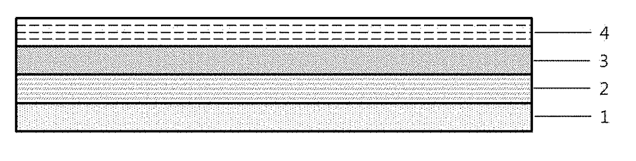
A conductive transparent film
a technology of conductive transparent film and conductive layer, which is applied in the manufacture of conductive layers, metallic material coating processes, cables/conductor components, etc., can solve the problems of not meeting the technical demand, increasing the specific resistance of the ito layer, and further delay in the reaction time of the conductive transparent film, so as to improve mechanical properties and response speed, excellent transmittance
- Summary
- Abstract
- Description
- Claims
- Application Information
AI Technical Summary
Benefits of technology
Problems solved by technology
Method used
Image

Examples
example 1
[0063]A solution containing a condensable organosilane compound (methyltrimethoxysilane) was coated on a transparent PET base material having a thickness of 50 μm and thermally cured to form an undercoating layer having a thickness of 40 nm. An anti-crack buffer layer comprising niobium oxide (NbOx) was deposited on the undercoating layer to a thickness of 1 nm by using a sputtering technique, while targeting niobium (Nb) and supplying a mixed gas of argon and oxygen to the deposition equipment. Similarly, an indium oxide layer comprising SnO2 was formed to a thickness of 21.3 nm on the anti-crack buffer layer using the sputtering technique to prepare a conductive transparent film. The constitution and physical properties of the prepared film are as shown in Tables 1 and 2, respectively.
examples 2 to 5
[0064]As shown in the following Table 1, a film was prepared in the same manner as in Example 1, except for the thickness of the anti-crack buffer layer and the surface resistance value. The physical properties of the prepared film are as shown in Table 2.
PUM
| Property | Measurement | Unit |
|---|---|---|
| thickness | aaaaa | aaaaa |
| thickness | aaaaa | aaaaa |
| thickness | aaaaa | aaaaa |
Abstract
Description
Claims
Application Information