
Semiconductor device and method for producing the same

a technology of semiconductor devices and semiconductors, applied in semiconductor devices, semiconductor/solid-state device details, electrical apparatus, etc., can solve the problems of short circuit between solder balls, reduced stiffness and thickness of circuit boards, and reduced stiffness of circuit boards, etc., to achieve high mounting reliability

Inactive Publication Date: 2006-04-27
PANASONIC CORP
View PDF10 Cites 107 Cited by
  • Summary
  • Abstract
  • Description
  • Claims
  • Application Information

AI Technical Summary

Benefits of technology

[0011] Therefore, with the foregoing in mind, it is an object of the present invention to provide a semiconductor device that is unlikely to cause warping and deformation and has high mounting reliability, and a method for producing the same.

Problems solved by technology

Moreover, when the connection pitch is set to be 0.5 mm or less for the purpose of downsizing the semiconductor device, a short circuit may occur between solder balls.
Furthermore, since the circuit boards are required to be flat and parallel to each other for solder connection, there are considerable limitations on the stiffness and thickness of the circuit boards.
However, since the cavity is formed in the vicinity of the semiconductor element, the stiffness of the circuit board will deteriorate when a thin resin substrate is used, and thus warping or deformation may occur easily.
Therefore, according to the above-mentioned configuration, mounting reliability of the semiconductor element and mounting reliability of the semiconductor device with respect to a mother board may deteriorate.
However, since the semiconductor element is in a built-in state in the core layer, thermal stress occurring at the joint between the semiconductor element and the substrate will be increased, and thus mounting reliability in a heat cycle test or a reflow test after moisture absorption will deteriorate considerably.
When the core layer is made of a low-elastic material for relieving the thermal stress, the strength of the core layer will deteriorate so that warping and deformation may occur easily.

Method used


Image

  • Semiconductor device and method for producing the same
  • Semiconductor device and method for producing the same
  • Semiconductor device and method for producing the same

Examples


embodiment 1

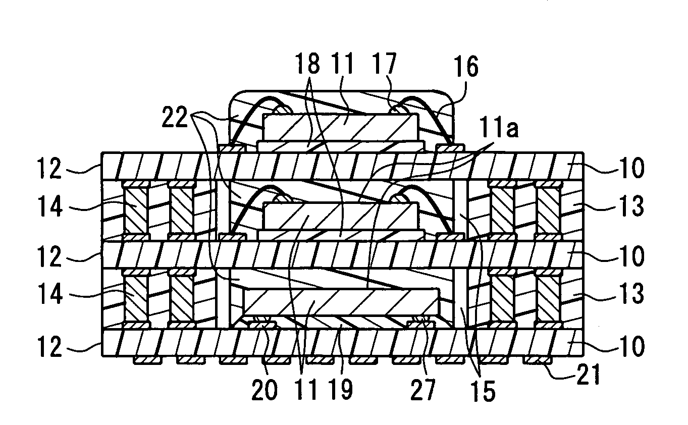
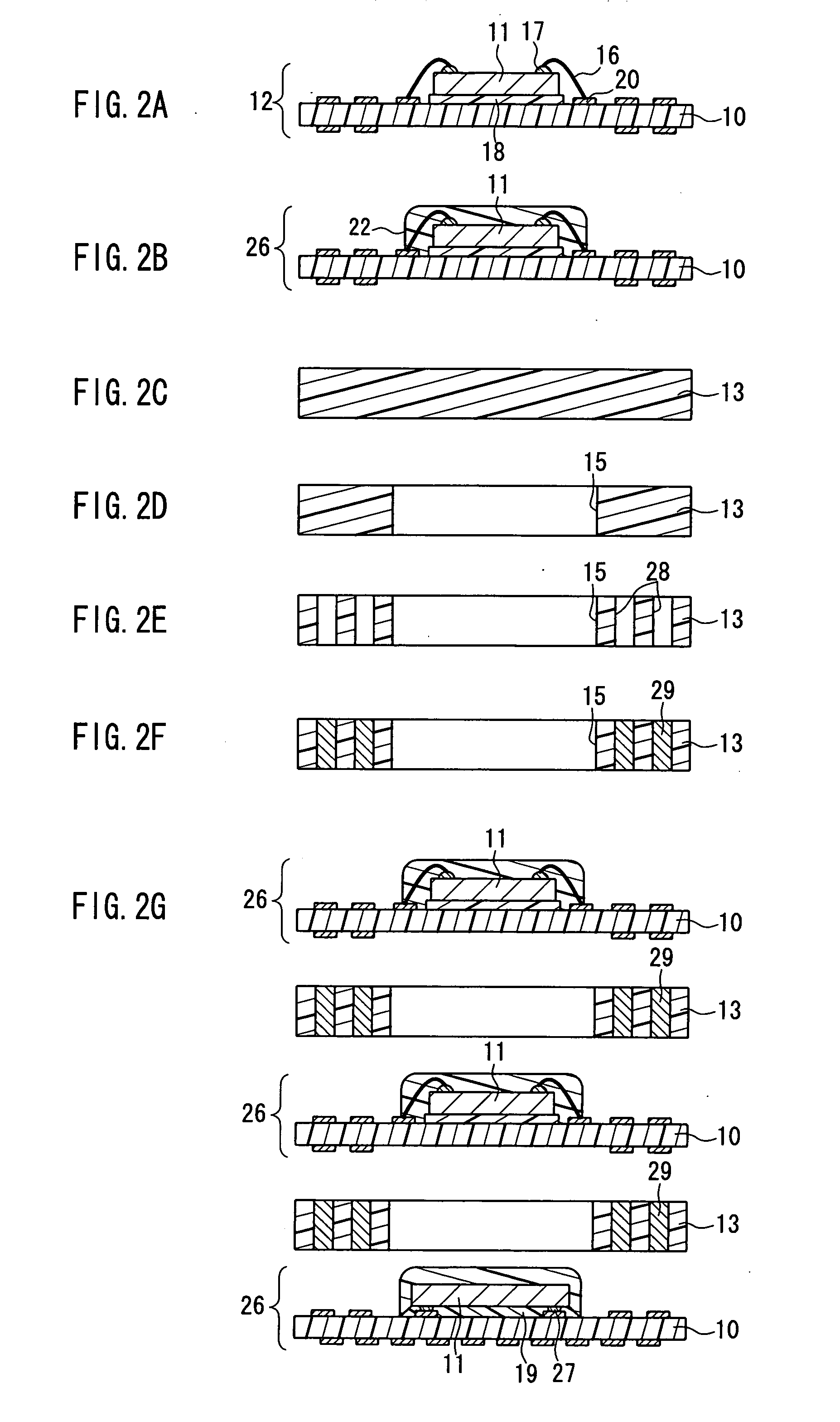
[0062]FIG. 1 is a cross-sectional view showing a semiconductor device according to Embodiment 1 of the present invention. As shown in FIG. 1, a semiconductor device according to Embodiment 1 has three circuit boards 12 including substrates 10 and semiconductor elements 11 mounted on the substrates 10, and these three circuit boards 12 are bonded to each other through sheet members 13 made of a thermosetting resin composition. The three circuit boards 12 are connected electrically with via-conductors 14 penetrating the sheet members 13, and the semiconductor elements 11 arranged between the substrates 10 are contained in element-containing portions 15. In FIG. 1, 16 denotes a wire, 17 denotes an electrode, 18 denotes a die-bond agent, 19 denotes an underfill, 20 denotes an element-mounting electrode, 21 denotes an external connection electrode, and 27 denotes a gold bump.

[0063] There is no particular limitation for the semiconductor elements 11, but semiconductor elements made of, f...

embodiment 2

[0089]FIG. 3 is a cross-sectional view showing a semiconductor device according to Embodiment 2 of the present invention. As shown in FIG. 3, in a semiconductor device according to Embodiment 2, all of the semiconductor elements 11 are flip-chip mounted. In the top and intermediate substrates 10 in FIG. 3, through holes 24 for communicating with element-containing portions 15 are formed, and penetration conductor 25 for electrically connecting the wirings formed on both the surfaces of the substrates 10 is formed on the through holes 24. A low-elastic material 22 is filled in the cavities in the element-containing portions 15. Namely, the semiconductor device according to Embodiment 2 has no cavities in the interior. Excepting this, the semiconductor device in this embodiment is similar to the semiconductor device (see FIG. 1) according to the above-mentioned Embodiment 1.

[0090] Since the above-mentioned through holes 24 are formed in the semiconductor device according to Embodimen...

embodiment 3

[0098]FIG. 5 is a cross-sectional view showing a semiconductor device according to Embodiment 3 of the present invention. As shown in FIG. 5, in a semiconductor device according to Embodiment 3, four circuit boards 12 are laminated. Through holes 24 are formed in all of the substrates 10 and provided with penetration conductors 25. Furthermore, on each of the bottom substrate 10 and a substrate 10 second from the bottom, a semiconductor element 11 to be contained in the element-containing portion 15 is mounted. The pair of semiconductor elements 11 are contained facing each other in the element-containing portion 15. A low-elastic material 22 is filled in the cavity in the element-containing portion 15 including space between surfaces 11a, 11a of the semiconductor elements 11, 11. Excepting these characteristics, the semiconductor device is similar to the above-mentioned semiconductor device (see FIG. 3) according to Embodiment 2. Therefore, the semiconductor device according to Emb...


PUM


Abstract

In a semiconductor device, circuit boards are connected electrically to each other by via-conductors that penetrate sheet members, semiconductor elements arranged between substrates are contained in element-containing portions formed on the sheet members, and a low-elastic material whose elastic modulus is lower than the elastic modulus of the thermosetting resin composition of the sheet members is filled in the space between the semiconductor elements contained in the element-containing portions and the substrates opposing surfaces opposite to the mounting surfaces of the semiconductor elements. Thereby, a semiconductor device resistant to warping and deformation and having a high mounting reliability is provided.

Description

BACKGROUND OF THE INVENTION [0001] 1. Field of the Invention [0002] The present invention relates to a semiconductor device used in an electric / electronic apparatus, and a method for producing the same. [0003] 2. Description of Related Art [0004] Due to an accelerated tendency toward miniaturization of portable electronic apparatuses, there is a keen demand for downsizing and high-density mounting of electronic parts to be incorporated. Among various electronic parts, semiconductor devices having multi-staged structures of laminating circuit boards including semiconductor elements have been proposed particularly. [0005] For an example of such semiconductor devices having multi-staged structures, JP H10-135267A proposes a semiconductor device including circuit boards that are electrically connected to each other with solder balls. [0006] However, since such a semiconductor device is formed by laminating a plurality of packaged circuit boards, the overall thickness of the semiconducto...

Claims


Application Information

Patent Timeline
Patent Type & Authority Applications(United States)
IPC IPC(8): H01L23/02
CPCH01L21/563H01L23/3121H01L23/5389H01L25/105H01L2224/16225H01L2224/32225H01L2224/48091H01L2224/48227H01L2224/48465H01L2224/73204H01L2224/73265H01L2224/83192H01L2924/01046H01L2924/01078H01L2924/01079H01L2924/09701H01L24/48H01L2924/01019H01L2224/45144H01L2224/73253H01L2924/3511H01L2225/1023H01L2225/107H01L2924/15311H01L24/45H01L2224/45015H01L2224/45124H01L2924/00014H01L2924/00H01L2924/00012H01L24/73H01L2924/181H01L2924/1627H01L2924/00011H05K3/4697H05K1/186H05K3/4069H01L2924/20752H01L2224/0401
Inventor HIRANO, KOICHINAKATANI, SEIICHISHIRAISHI, TSUKASAHAYASHI, YOSHITAKE
Owner PANASONIC CORP
Features
  • Generate Ideas
  • Intellectual Property
  • Life Sciences
  • Materials
  • Tech Scout
  • Unparalleled Data Quality
  • Higher Quality Content
  • 60% Fewer Hallucinations
Learn More