Built-up substrate, method for manufacturing same, and semiconductor integrated circuit package

a technology manufacturing methods, applied in the direction of printed circuit aspects, lithography/patterning, cable/conductor manufacturing, etc., can solve the problems of difficult mounting of semiconductor integrated circuits on package wiring substrates, difficult to mount semiconductor integrated circuits in large sizes, and difficult to mount ceramic substrates in large sizes. , to achieve the effect of improving the position accuracy of the via hole, easy formation, and excellent insulation reliability

Active Publication Date: 2014-05-08
PANASONIC INTELLECTUAL PROPERTY MANAGEMENT CO LTD
View PDF6 Cites 16 Cited by
  • Summary
  • Abstract
  • Description
  • Claims
  • Application Information

AI Technical Summary

Benefits of technology

[0027]The manufacturing method of a build-up substrate according to the present invention uses the “photosensitive metal oxide precursor material”, which can result in the thin build-up insulating film with excellent reliability of insulation. The “photosensitive metal oxide precursor material” may be the material in the form of paste or liquid, and thus may be applied by the spray method or slit coaster method, which can easily achieve the formation of the film in a uniform thickness over the substrate having a large size. The coated film (more specifically, “insulating film obtained by drying after application”) is made of the “photosensitive metal oxide precursor material” and thus can be exposed and developed at one time. As a result, the via holes can be collectively processed. Thus, the positional accuracy of the via holes can be improved. That is, the via holes having a small diameter can be easily formed even in the large-sized substrate at low cost.
[0028]The manufacturing method of the present invention in the present application has a high flexibility in selection of the circuit substrate for the core because the heating temperature for obtaining the metal oxide precursor film is relatively low. For example, the build-up substrate can have the desired elastic modulus or bending property depending on the type of the core substrate. By way of example, when the insulating material of the circuit substrate (insulating base) as the core is made of organic material, the build-up substrate can be obtained which can exhibit some bending property, and which has the high reliability of insulation and high flexibility. In contrast, when the insulating material of the circuit substrate (insulating base) as the core is made of inorganic material, all the build-up insulating layers and the build-up wiring patterns can be substantially formed of inorganic material. Thus, the build-up substrate can improve the reliability as the substrate, and can also have the high reliability of mounting because its thermal expansion coefficient is substantially similar to that of a silicon semiconductor.
[0029]Further, the present invention can provide the dense build-up insulating layer that can have the high elastic modulus even in a very small thickness of 1 μm or more and 20 μm or less because the insulating layer is formed of the “metal oxide inorganic film”, and hence achieves the thin semiconductor package suitable for use in mobile devices.
[0030]The build-up substrate of the present invention has the high elasticity and adequate thermal expansion even when the substrate is small in thickness and large in size, which can suppress the break or cracking of the build-up substrate. Therefore, the present invention can suitably manufacture the build-up substrate using a manufacturing infrastructure of a printed board.

Problems solved by technology

With the miniaturization and increase in number of the I / O terminals at the same time, the miniaturization or decrease of a terminal pitch is further progressed, which makes it difficult to mount a semiconductor integrated circuit on a package wiring substrate.
However, the ceramic substrate is difficult to fire in a large size.
It tends to cause cracks, and thus, the ceramic substrate is not appropriate for thinning.
The use of such a large-sized chip causes warpage of even the normal build-up substrate during a manufacturing process or due to a heat history during mounting of a LSI chip, which might peel off a soldered portion of a joint.
Additionally, the miniaturization of a small-sized via hole process or a fine wiring pitch reduces the insulating reliability, which might decrease the withstand voltage or cause insulating failure.

Method used


Image

  • Built-up substrate, method for manufacturing same, and semiconductor integrated circuit package
  • Built-up substrate, method for manufacturing same, and semiconductor integrated circuit package
  • Built-up substrate, method for manufacturing same, and semiconductor integrated circuit package

Examples


first embodiment

Manufacturing Process of First Embodiment

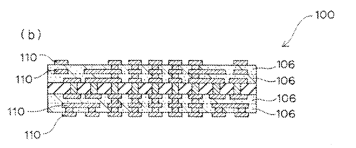
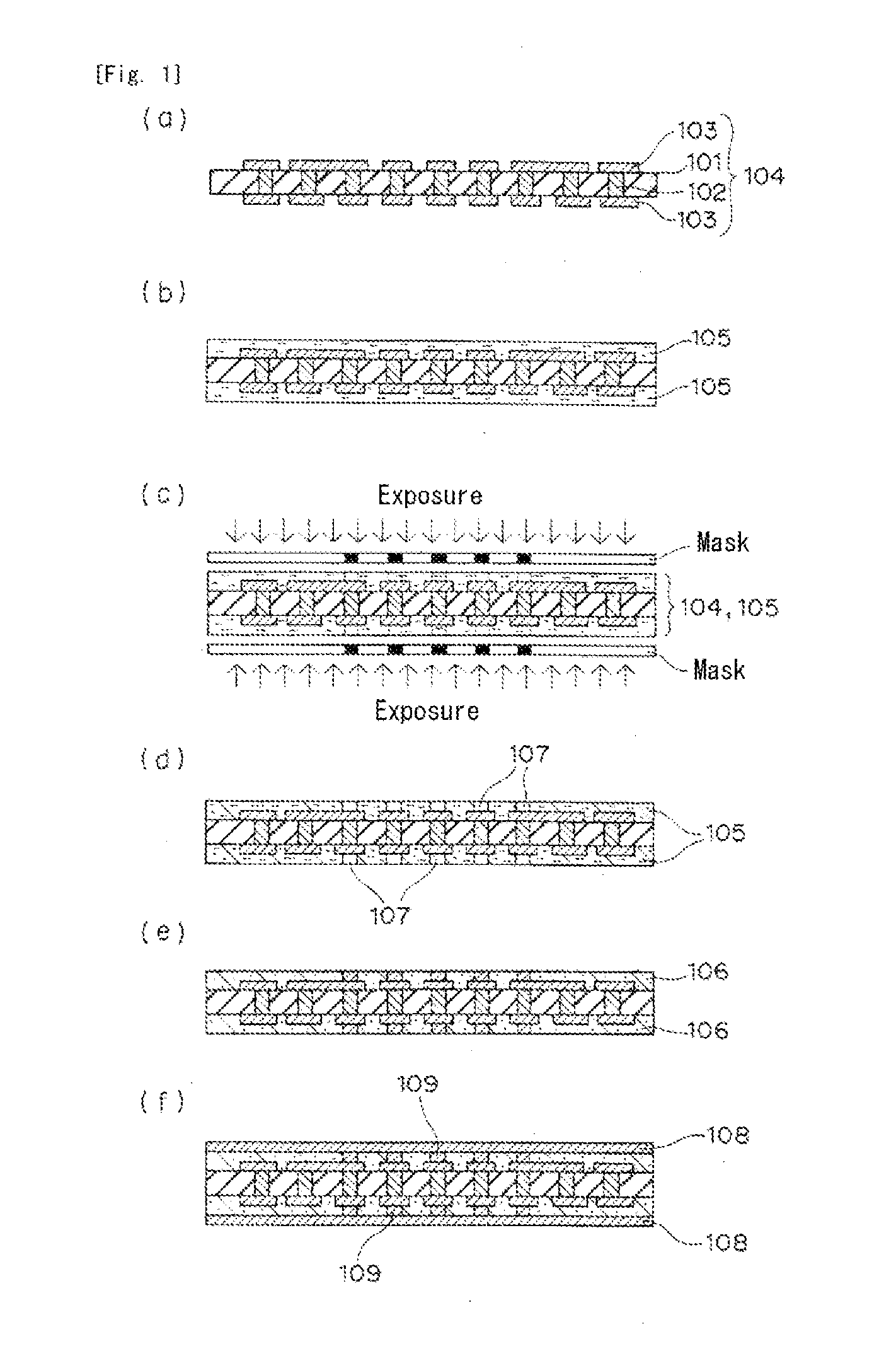
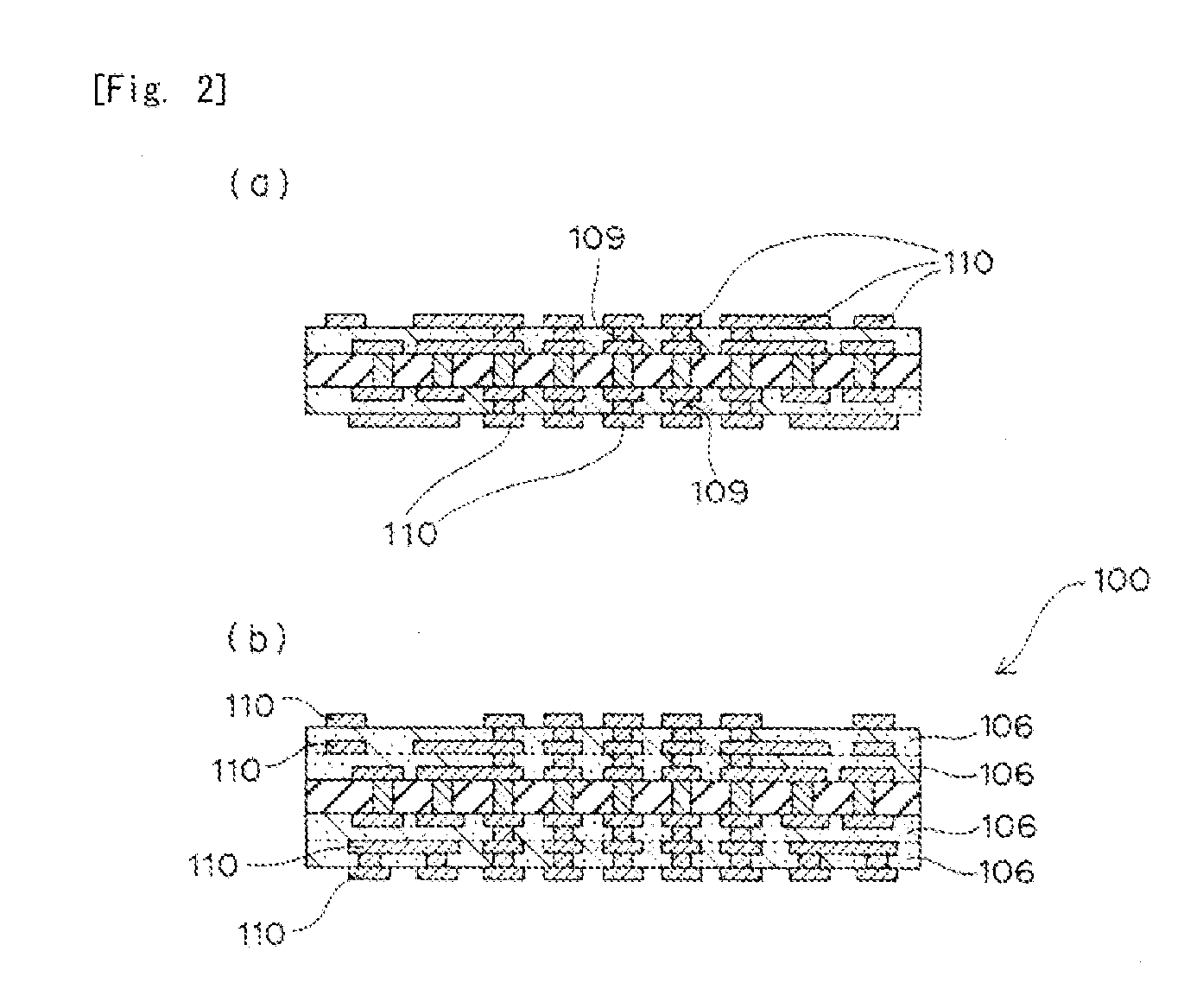
[0046]A manufacturing method of a build-up substrate according to a manufacturing process of a first embodiment of the present invention will be described below with reference to FIGS. 1 and 2.

[0047]In performing the manufacturing method of the present invention, first, step (i) is performed. That is, a photosensitive metal oxide precursor material is applied to one or both sides of a circuit substrate including a wiring pattern, and then the applied material is dried to form an insulating film. Specifically, as shown in FIG. 1(a), a circuit substrate 104 is provided which has wiring patterns 103 on both or one side thereof. For example, the circuit substrate 104 with the wiring patterns 103 on its both sides can be obtained in the following way. That is, a metal layer made of a copper foil is laminated on each side of a base 101 formed by immersing a glass woven fabric in an epoxy resin. Then, the base with the metal layers are heated and pr...

second embodiment

Manufacturing Process of Second Embodiment

[0067]Next, another manufacturing method of a build-up substrate according to a manufacturing process of a second embodiment of the present invention will be described below with reference to FIGS. 5 and 6 (note that the same features as those in the “manufacturing process of the first embodiment” will be omitted in principle to avoid the redundant description).

[0068]First, as shown in FIG. 5(a), a release carrier 500 is provided. The release carrier 500 is finally to be removed. The release carrier 500 for use can be an organic film which is easily peeled off, for example, an organic film made of PET or PPS. In another method, the release carrier 500 for use can be a metal foil which is chemically dissolved and removed, for example, a copper foil. The carrier 500 preferably has enough thickness, for example, of 80 to 120 μm, to withstand handling as a carrier during transportation including the following steps. As shown in FIG. 5(b), wiring...

third embodiment

Manufacturing Process of Third Embodiment

[0069]Next, another manufacturing method of a build-up substrate according to a manufacturing process of a third embodiment of the present invention will be described below with reference to FIGS. 7(a) to 7(h) (note that the same features as those in the “manufacturing process of the first embodiment” and the “manufacturing process of the second embodiment” will be omitted in principle to avoid the redundant description).

[0070]The manufacturing process of the third embodiment involves step (iv)′ instead of the above step (iv). In the process of step (iv)′, after forming a resist on the surface of the build-up insulating layer, the build-up insulating layer and the resist are subjected to plating as a whole. Finally, the resist is removed, which produces via holes and build-up wiring patterns in parts without resist.

[0071]First, as shown in FIGS. 7(a) to 7(c), the above steps (i) to (iii) are performed. That is, a photosensitive metal oxide pr...


PUM


Abstract

A method for manufacturing a build-up substrate, the build-up substrate comprising an insulating layer and a wiring pattern layer stacked over a circuit substrate, said method comprising the steps of: (i) applying a photoactive metal oxide precursor material to one or both sides of the circuit substrate with a wiring pattern, and drying the applied photoactive metal oxide precursor material to form an insulating film; (ii) forming an opening for a via hole in the insulating film by exposure and development of the insulating film; (iii) applying a heat treatment to the insulating film to convert the insulating film into a metal oxide film, thereby forming a build-up insulating layer of the metal oxide film; and (iv) plating the build-up insulating layer to form via holes in the openings, forming a metal layer on the build-up insulating layer, and etching the metal layer to form a build-up wiring pattern; and (v) repeating the steps from (i) to (iv) at least one time.

Description

TECHNICAL FIELD[0001]The present invention relates to build-up substrates, manufacturing methods thereof, and semiconductor integrated circuit packages. More particularly, the present invention relates to a build-up substrate including a build-up insulating layer substantially formed of inorganic material, and a method for manufacturing the build-up substrate. Further, the present invention also relates to a semiconductor integrated circuit package that can be obtained from the build-up substrate.BACKGROUND OF THE INVENTION[0002]The development of electronic devices contributes to the speeding up of the operation of semiconductor integrated circuits (LSI) used in a CPU or GPU of a computer, a digital television, a smartphone, and the like. Particularly, image processing LSI or the like is being speeded up and highly integrated, and thus is desired to further reduce its size or respond to the increase in number of I / O terminals.[0003]With the miniaturization and increase in number of...

Claims


Application Information

Patent Timeline
Patent Type & Authority Applications(United States)
IPC IPC(8): H01L23/498H05K1/03H01L21/48
CPCH01L23/49822H05K1/0313H05K1/0306H01L21/4857H01L23/15H01L23/3731H01L23/49827H01L2224/16225H05K3/4673H05K3/4682H05K2201/017H05K2201/0175H05K2203/0126H05K2203/0514H05K2203/1366
Inventor NAKATANI, SEIICHIKAWAKITA, KOJISAWADA, SUSUMUYAMASHITA, YOSHIHISA
Owner PANASONIC INTELLECTUAL PROPERTY MANAGEMENT CO LTD
Why Eureka
Try Eureka