Conductive connecting material, method for producing electronic component, electronic member with conductive connecting material and electronic component

a technology of conductive connecting material and electronic component, which is applied in the direction of printed circuit assembling, solid-state devices, synthetic resin layered products, etc., can solve the problems of difficult to further narrow the pitch between the adjacent terminals, the insulation properties of the adjacent terminal cannot be sufficiently ensured, and the difficulty of controlling the aggregation of conductive particles, etc., to achieve excellent electrical connection, facilitate connection, and high insulation reliability

Inactive Publication Date: 2012-10-18
SUMITOMO BAKELITE CO LTD
View PDF9 Cites 15 Cited by
  • Summary
  • Abstract
  • Description
  • Claims
  • Application Information

AI Technical Summary

Benefits of technology

[0014]According to the present invention, it is possible to provide a conductive connecting material that ensures excellent electrical connection between opposed terminals and high insulation reliability between adjacent terminals, and facilitates connection between electronic members having a plurality of terminals and formation of connecting terminals on an electrode of an electronic member.

Problems solved by technology

However, in the existing anisotropic conductive adhesive or anisotropic conductive film, it is extremely difficult to control aggregation of conductive particles.
Therefore, there are problems such that (1) a part of opposed terminals is not conducted since a conductive particle and a terminal or conductive particles do not sufficiently contact to each other, and (2) conductive particles remain in the resin (insulating areas) positioned in areas other than those between opposed terminals (conductive areas) to cause a leak current and therefore the insulation properties between adjacent terminals cannot be sufficiently ensured in some cases.
Therefore, it is difficult to further narrow the pitch between terminals by using conventional anisotropic conductive adhesive or anisotropic conductive film.
However, in this method, when the pitch between connecting terminals is narrow, the cost of a mask used for printing the solder paste is increased.
Furthermore, when the size of the connecting terminal is extremely small, printing of the solder paste may be impossible in some cases.
However, in this method, when the connecting terminal is extremely small, the cost involved in producing the solder ball is increased and it is technically difficult to produce a small sized solder ball in some cases.

Method used


Image

  • Conductive connecting material, method for producing electronic component, electronic member with conductive connecting material and electronic component
  • Conductive connecting material, method for producing electronic component, electronic member with conductive connecting material and electronic component
  • Conductive connecting material, method for producing electronic component, electronic member with conductive connecting material and electronic component

Examples


first embodiment

(1) First Embodiment

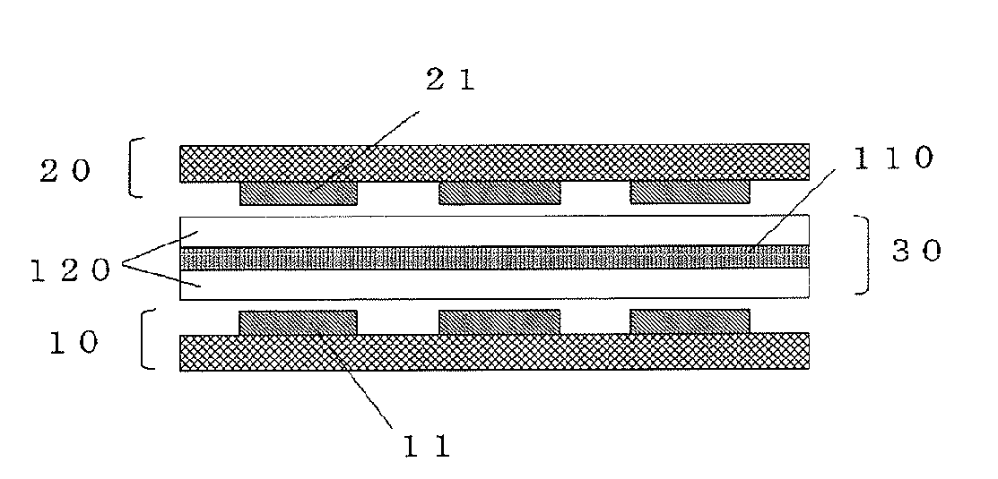
[0174]In the second method for producing an electronic component according to the first embodiment of the present invention, the step of forming conductive portions is carried out by heating the conductive connecting material at a temperature of equal to or more than the melting point of the metal layer and a temperature at which curing of the resin layer is not completed, while the step of curing or solidifying the resin layer is carried out by heating the conductive connecting material at a temperature at which curing of the resin layer is completed.

[0175]In this second method for producing an electronic component, it is possible to selectively aggregate the heated and melted metal layer on the electrode on the substrate to form a connecting terminal, and to form an insulating area by the curable resin composition around the connecting terminal. As a result, the periphery of the connecting terminal is covered with the curable resin composition, and therefore th...

second embodiment

(2) Second Embodiment

[0186]Hereinafter, the second method for producing an electronic component according to the second embodiment of the present invention will be described.

[0187]In the second method for producing an electronic component according to the second embodiment of the present invention, the step of forming conductive portions is carried out by heating the conductive connecting material at a temperature of equal to or more than the melting point of the metal layer and a temperature at which the resin layer is softened, while the step of curing or solidifying the resin layer is carried out by cooling the conductive connecting material to a temperature at which the resin layer is solidified.

[0188]In the production method of the second embodiment, it is possible to selectively aggregate the heated and melted metal layer on the electrode on the substrate to form a connecting terminal, and to form an insulating area by the thermoplastic resin composition around the connecting ...

examples

[0201]The present invention is now illustrated below with reference to Examples. However, the present invention is not restricted to the following Examples.


PUM

PropertyMeasurementUnit
particle diameteraaaaaaaaaa
temperatureaaaaaaaaaa
melting pointaaaaaaaaaa

Abstract

Disclosed is a conductive connecting material 30 used to form conductive portions on a plurality of terminals 11 of an electronic member having a substrate 10 and the plurality of terminals 11 provided on the substrate 10, comprising a metal layer 110 and a resin layer 120 having a resin component and a filler, in which the metal layer is aggregated on each of terminals to form the conductive portions on the plurality of terminals by bringing the conductive connecting material into contact with the plurality of terminals and heating the conductive connecting material.

Description

TECHNICAL FIELD[0001]The present invention relates to a conductive connecting material, a method for producing an electronic component, an electronic member with the conductive connecting material and an electronic component.BACKGROUND ART[0002]In recent years, with the requirements of higher functionality and reduction in a size of electronic devices, the pitch between connecting terminals in an electronic material has been more and more narrowed, and connection between terminals in a fine pitch circuit has also been sophisticated. As a method for connecting terminals, for example, a flip-chip connection technique, in which, when an IC chip is electrically connected to a circuit board, an anisotropic conductive adhesive or anisotropic conductive film is used to connect a plurality of terminals at one time, has been known. Such an anisotropic conductive adhesive or anisotropic conductive film is a film or a paste in which conductive particles are dispersed in an adhesive containing ...

Claims


Application Information

Patent Timeline
Patent Type & Authority Applications(United States)
IPC IPC(8): H05K7/02B32B27/42B32B15/098B32B5/16H05K1/11F27D3/00
CPCC08L63/00Y10T428/25H01L2924/14H01L2924/3025H05K3/3478H05K3/3489H05K3/4007H05K2203/0405H05K2203/0425H05K2203/043H01L24/26H01L2924/01012H01L2924/01029H01L2924/07811C09J9/02H01L2924/00H01L24/11H01L24/13H01L24/29H01L24/32H01L24/83H01L2224/04026H01L2224/05568H01L2224/1152H01L2224/29012H01L2224/29076H01L2224/29083H01L2224/29109H01L2224/29111H01L2224/29113H01L2224/29116H01L2224/2912H01L2224/29124H01L2224/29139H01L2224/29144H01L2224/29147H01L2224/29155H01L2224/2916H01L2224/2919H01L2224/73104H01L2224/83191H01L2224/83192H01L2224/83205H01L2224/83222H01L2224/83801H01L2224/83862H01L2224/83885H01L2224/83886H01L2924/12042Y10T428/31678Y10T428/31688H01L2924/00014H01L2924/00012H01B5/02H01R11/01H05K3/34
Inventor CHUMA, TOSHIAKIKAGIMOTO, TOMOHIRO
Owner SUMITOMO BAKELITE CO LTD
Why Eureka
Try Eureka