Adhesive film for producing semiconductor device
- Summary
- Abstract
- Description
- Claims
- Application Information
AI Technical Summary
Benefits of technology
Problems solved by technology
Method used
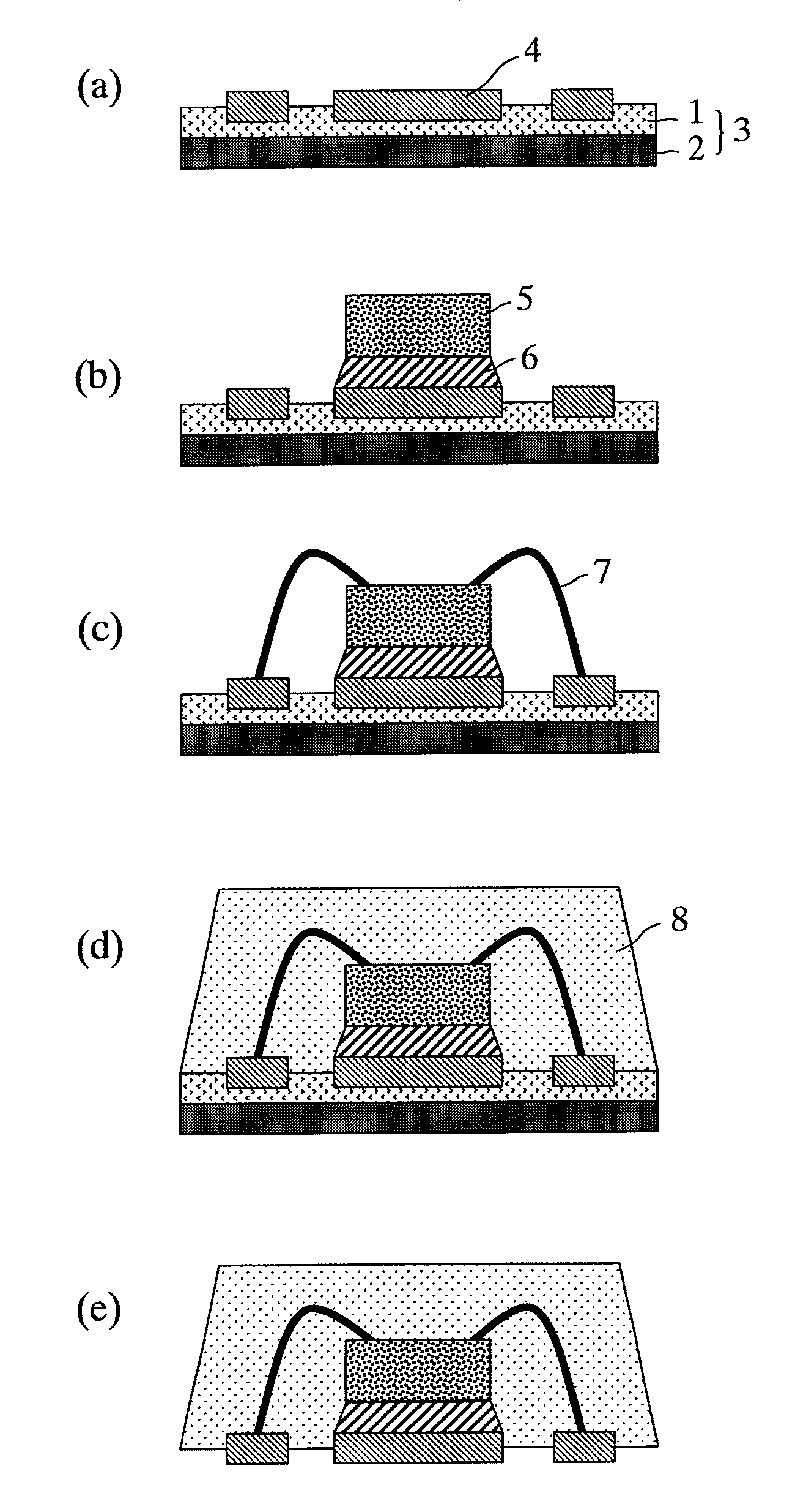
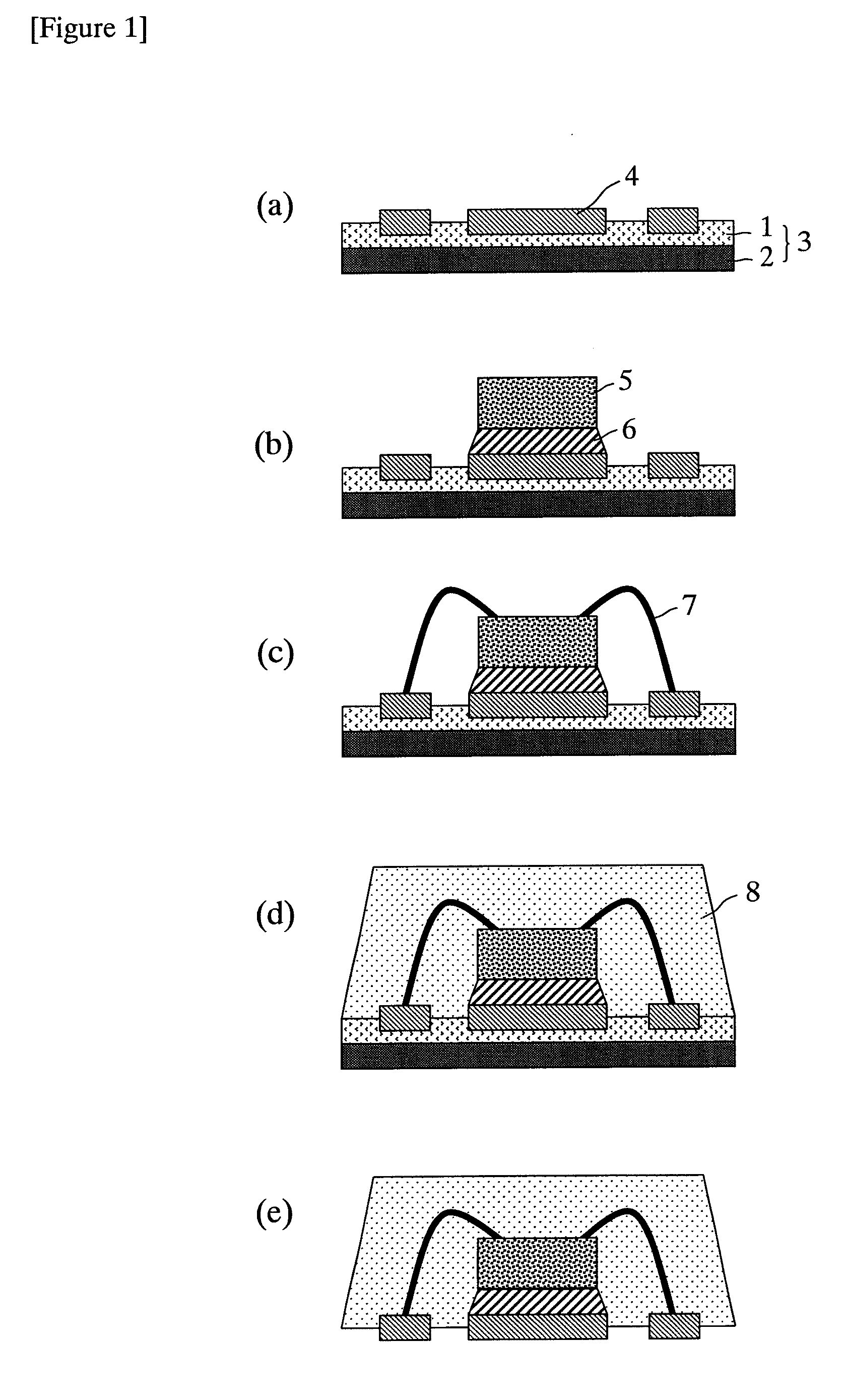
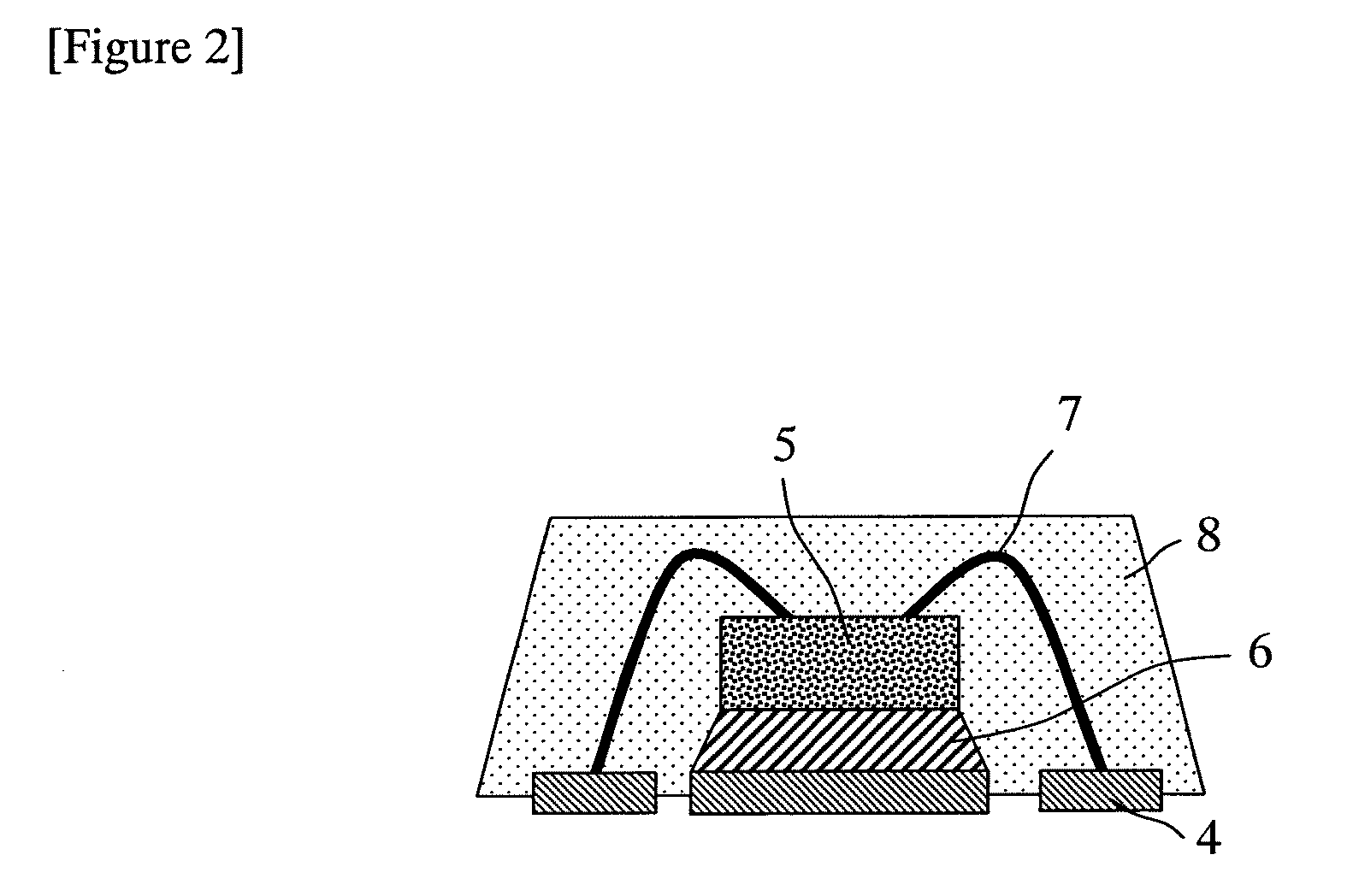
Image

Examples
example 1
[0055]Thirty parts by weight of acrylonitrile-butadiene rubber (“Nipol 1072J” manufactured by ZEON CORPORATION; content of acrylonitrile: 18% by weight), 1.5 parts by weight of a layered clay mineral (Somasif MAE, manufactured by CO-OP Chemical, swellable mica, average plane distance: 32 Å, average particle size (D50): 5 to 7 μm, aspect ratio (thickness: 1 nm): 5000 to 7000), 65 parts by weight of bisphenol A epoxy resin (“Epikote 828” manufactured by Japan Epoxy Resins Co., Ltd.; epoxy equivalent: 190 g / eq), and 5 parts by weight of imidazole (“C11Z” manufactured by Shikoku Kasei K.K.) were mixed together, and the components were dissolved in a methyl ethyl ketone solvent so as to have a solid content of 35% by weight, to give a thermosetting adhesive solution. The resulting thermosetting adhesive solution was applied onto a copper foil having a thickness of 100 μm as a heat-resistant backing, and then dried at 150° C. for 3 minutes, thereby forming a thermosetting adhesive layer h...
example 2
[0058]The adhesive film was produced in the same manner as in Example 1 except that the amount of a layered clay mineral added was changed to 3 parts by weight. The adhesive strength of the adhesive film to the copper foil after curing the adhesive film was 8.8 N / 20 mm at 23° C.
example 3
[0059]The adhesive film was produced in the same manner as in Example 1 except that the amount of a layered clay mineral added was changed to 6 parts by weight. The adhesive strength of the adhesive film to the copper foil after curing the adhesive film was 9.5 N / 20 mm at 23° C.
PUM
| Property | Measurement | Unit |
|---|---|---|
| Percent by mass | aaaaa | aaaaa |
| Percent by mass | aaaaa | aaaaa |
| Percent by mass | aaaaa | aaaaa |
Abstract
Description
Claims
Application Information
 - Generate Ideas
- Intellectual Property
- Life Sciences
- Materials
- Tech Scout
- Unparalleled Data Quality
- Higher Quality Content
- 60% Fewer Hallucinations
Browse by: Latest US Patents, China's latest patents, Technical Efficacy Thesaurus, Application Domain, Technology Topic, Popular Technical Reports.
© 2025 PatSnap. All rights reserved.Legal|Privacy policy|Modern Slavery Act Transparency Statement|Sitemap|About US| Contact US: help@patsnap.com