Semiconductor memory

a semiconductor and memory technology, applied in the field of semiconductor memory, can solve the problem of inability to form a non-uniform pattern in the extended region, and achieve the effect of avoiding the formation of uniform patterns

Active Publication Date: 2006-04-13
KATANA SILICON TECH LLC
View PDF6 Cites 36 Cited by
  • Summary
  • Abstract
  • Description
  • Claims
  • Application Information

AI Technical Summary

Problems solved by technology

Therefore, it is impossible to form a non-uniform pattern in the extended region.
This problem brings about needs to form contacts within such a pattern of lines and spaces not including such contact formation patterns.

Method used


Image

  • Semiconductor memory
  • Semiconductor memory
  • Semiconductor memory

Examples


first embodiment

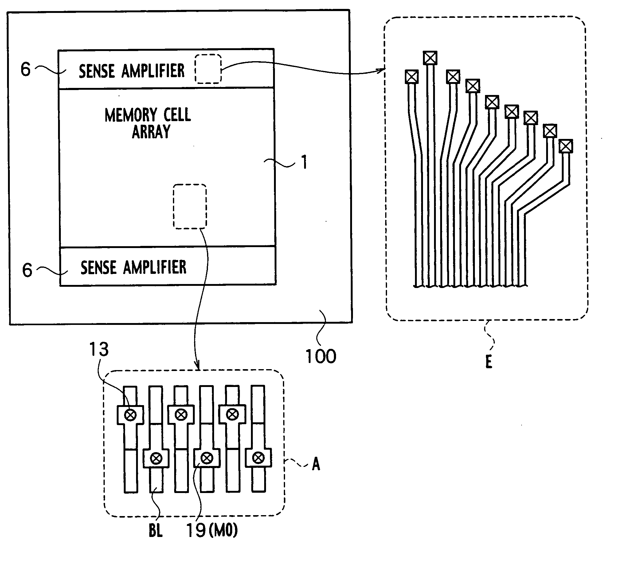
[0070] As shown in FIG. 19, a semiconductor memory according to the first embodiment of the present invention includes: multiple bit lines BLj−2, BLj−1, BLj, BLj+1, BLj+2, . . . (not shown in the drawing), which extend along the column length; multiple word lines WL1, WL2, . . . , which extend along the row length; and multiple word line contacts (borderless contacts CG) 14, which are formed at the ends of those word lines WL1, WL2, . . . , respectively; and have a structure where the word lines WL1, WL2, . . . are linearly arranged and the lengths of at least two adjacent word lines along the row length differ from each other.

[0071] Alternatively, the semiconductor memory is structured such that each of the word line contacts (borderless contacts CG) 14 is in contact with part of one of the multiple word lines WL1, WL2, . . . , but is not in contact with word lines adjacent to that one of the multiple word lines.

[0072] Alternatively, the semiconductor memory is structured such th...

first modified example

OF THE FIRST EMBODIMENT

[0087]FIG. 8 shows a plan view of a pattern for describing a step of a semiconductor memory fabrication method according to a first modified example of the first embodiment of the present invention; wherein 3L denotes the interval between a pair of select gate line SG1 patterns, which is prepared for bit line contacts (CB) 11. L denotes the minimum line and space (minimum line width) As shown with a dashed line in FIG. 8, a pattern structure of FIG. 8 may be achieved by removing only a single dummy interconnect DE through double exposure. For example, as shown in FIG. 8, the semiconductor memory, according to the first modified example of the first embodiment of the present invention, includes a contact forming region with dimensions three times the minimum line width L, which is formed by removing one of the multiple word line patterns and select gate line patterns through double exposure.

second modified example

OF THE FIRST EMBODIMENT

[0088]FIG. 9 shows a plan view of a pattern for describing a step of a semiconductor memory fabrication method, according to a second modified example of the first embodiment of the present invention, where 5L denotes the interval between the select gate line SG2 pattern and the select gate line SG1 pattern, which is prepared for bit line contacts (CB) 11. As shown with dashed lines in FIG. 9, a pattern structure of FIG. 9 may be achieved by removing only a single dummy interconnect DE and a single select gate line SG1 through double exposure. For example, as shown in FIG. 9, the semiconductor memory according to the second modified example of the first embodiment of the present invention, includes a contact forming region with dimensions five times the minimum line width L, which is formed by removing two of the multiple word line patterns and select gate line patterns through double exposure.


PUM


Abstract

Borderless contacts for word lines or via contacts for bit lines are formed using interconnect patterns, a part of which is removed. A semiconductor memory includes: a plurality of active regions AAi, AAi+1, . . . , AAn, which extend on a memory cell array along the column length; a plurality of word line patterns WL1, WL2, . . . , extend along the row length and are non-uniformly arranged; a plurality of select gate line patterns SG1, SG2, . . . , are arranged parallel to the plurality of word line patterns; borderless contacts are formed near the ends of the word line patterns on the memory cell array, and are in contact with part of an interconnect extended from the end of the memory cell array, but are not in contact with interconnects adjacent to that interconnect; and bit line contacts are formed within contact forming regions provided by removing part of the plurality of word line patterns and select gate line patterns through double exposure.

Description

CROSS REFERENCE TO RELATED APPLICATIONS AND INCORPORATION BY REFERENCE [0001] This application is based upon and claims the benefit of priority from prior Japanese Patent Application P2004-295268 filed on Oct. 7,2004; the entire contents of which are incorporated by reference herein. BACKGROUND OF THE INVENTION [0002] 1. Field of the Invention [0003] The present invention relates to interconnect layers and contacts in a semiconductor. More specifically, it relates to a semiconductor memory including an extended region, extended from a cell array, in which interconnects are formed at a fine pitch. A control gate, a metallic interconnect, a bit line pattern, or related patterns are formed with non-uniform patterns in such extended region. [0004] 2. Description of the Related Art [0005] Diagonal interconnects are conventionally used in extended regions of a semiconductor memory. More specifically, diagonal interconnects are used to provide a longer pitch in a region extending to contac...

Claims


Application Information

Patent Timeline
Patent Type & Authority Applications(United States)
IPC IPC(8): G11C5/06
CPCG11C5/063G11C16/0408H01L27/0207H01L27/105H01L27/11519H01L27/11526H01L27/11531H10B41/10H10B41/40H10B41/42H10B41/35
Inventor SUGIMAE, KIKUKOTANAKA, SATOSHIHASHIMOTO, KOJIICHIGE, MASAYUKI
Owner KATANA SILICON TECH LLC
Why Eureka
Try Eureka