

Method and its apparatus for classifying defects
a defect type and defect technology, applied in the field of methods and apparatus for classifying defects, can solve the problems of not being able to effectively use information on defects not reviewed, and being difficult to review all defects from time restrictions
- Summary
- Abstract
- Description
- Claims
- Application Information
AI Technical Summary
Benefits of technology
Problems solved by technology
Method used
Image

Examples
first embodiment
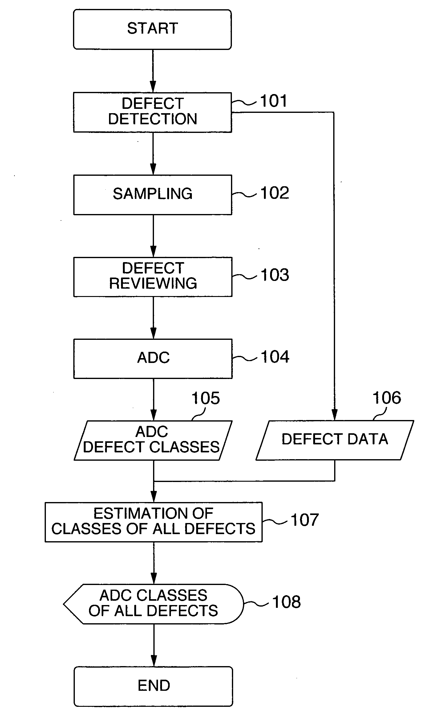
[0037]FIG. 1 is a flow chart illustrating processes of an automatic defect classifying method according to the first embodiment of the present invention. Defects on a wafer subjected to semiconductor manufacture processes and transported to an inspection process are detected with a conventionally well-known inspection equipment or the like (101). The inspection equipment calculates at least defect position coordinates and attribute amounts as information on defects (106). Defects to be reviewed are selected from the detected defects by conventionally well-known sampling (102).
[0038] Next, the selected defects are reviewed with a conventionally well-known SEM type review equipment or the like having a high resolution (103). Reviewed results are passed to a conventionally well-known ADC and classified into defect classes (104). In accordance with input defect classes 105 of ADC and defect data 106, defects not having defect classes of ADC are assigned the defect classes of ADC (107)....
second embodiment
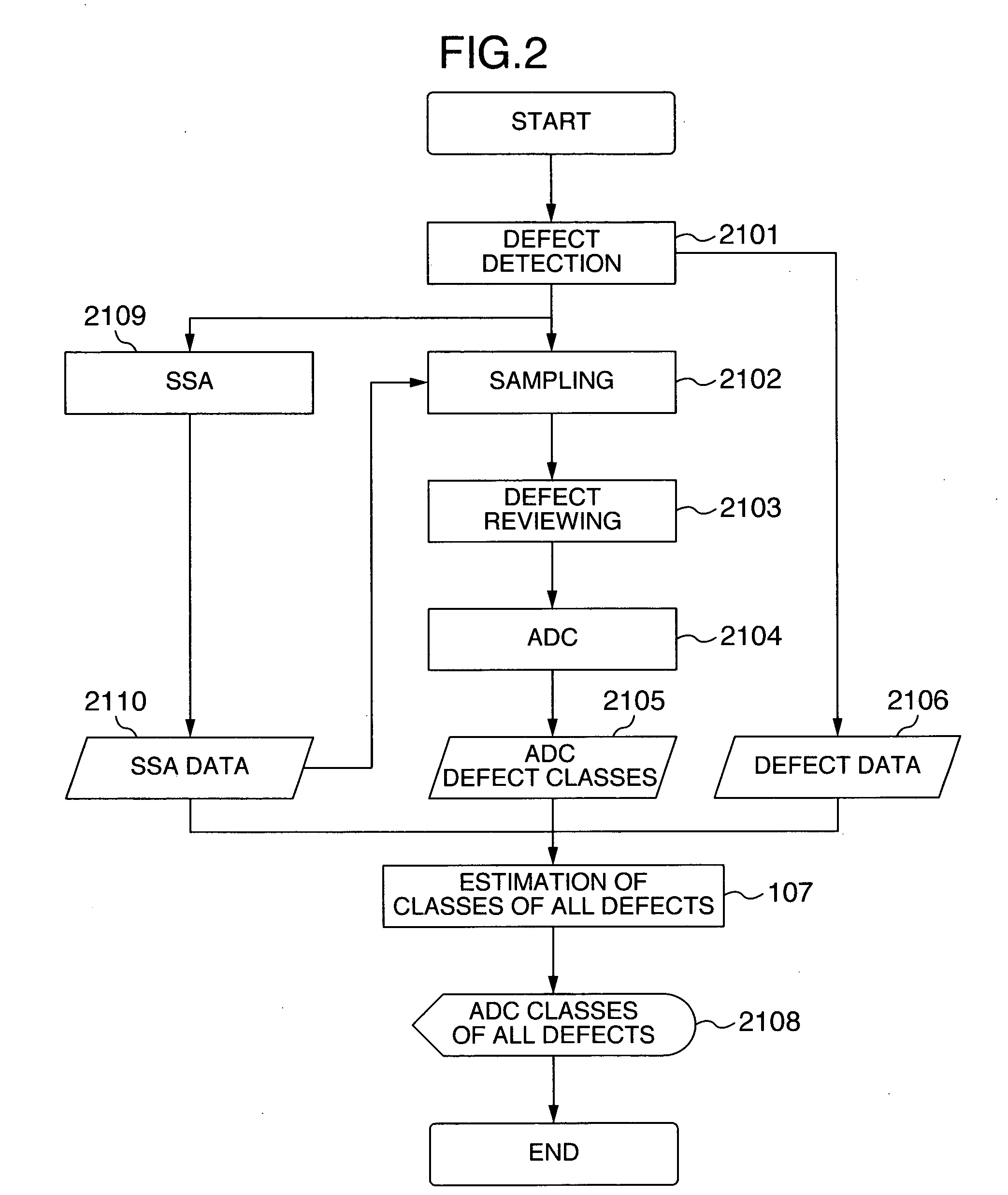
[0064]FIG. 2 shows the second embodiment of the invention.
[0065] In the second embodiment, steps from a defect detection 2101 to ADC defect classes 2105 are the same as the defect detection 101 to the ADC defect classes 105 shown in FIG. 1. A different point from the first embodiment resides in that after the defect detection 2101, a spatial signature analysis (SSA) 2109 is executed which analyzes the defect distribution state and SSA data 2110 of the analysis result is input to a sampling 2102 and a class estimation 2107 for all defects.
[0066] A defect distribution of a wafer is generally shifted because of performances specific to equipments and processes. SSA 2109 has been proposed to analyze the defect distribution state from defect position information on a wafer. For example, a method disclosed in JP-A-2003-059984 is used for SSA. According to this method, defects are classified into defects having an area of a defect distribution attribute class and random defects, dependin...
third embodiment
[0078]FIG. 3 illustrates the third embodiment.
[0079] In the third embodiment, steps from a defect detection 3101 to ADC defect classes 3105 are the same as the defect detection 101 to the ADC defect classes 105 shown in FIG. 1. A different point from the first embodiment resides in that before the defect detection 3101, a database is accessed 3111 to search computer aided design (CAD) data 3112 which is formed when chips in a semiconductor wafer are designed and describes the chip layout of two dimensions and a plurality of layers, and the searched data is input to a class estimation 3107 for all defects.
[0080] Defect data 3106 obtained by the defect detection 3101 has a smaller amount of information for classification than the information obtained by a defect review 3103, because a resolution of the inspection equipment is low. By using the CAD data 3112 of a wafer with defects, it becomes possible to obtain information on a pattern density, a pattern edge density and the like of...
PUM
 Abstract
Description
Claims
Application Information