Light emitting diode and lens for the same

a technology of light emitting diodes and lenses, applied in the direction of instruments, semiconductor devices for light sources, lighting and heating devices, etc., can solve problems such as problems

Active Publication Date: 2006-04-20
SAMSUNG DISPLAY CO LTD
View PDF13 Cites 172 Cited by
  • Summary
  • Abstract
  • Description
  • Claims
  • Application Information

AI Technical Summary

Benefits of technology

[0069] Here, it is preferable that an acute angle formed between a straight line linking the center of the base to a point of the curved central surface and the main axis of the lens is smaller than an acute angle formed between the normal for the corresponding point of the curved central surface and the main axis of the lens.

Problems solved by technology

However, some problems may arise when the LED is used as a surface light source device.

Method used


Image

  • Light emitting diode and lens for the same
  • Light emitting diode and lens for the same
  • Light emitting diode and lens for the same

Examples


Embodiment Construction

[0090] Preferred embodiments of the present invention will now be described more fully hereinafter with reference to the accompanying drawings, in which preferred embodiments of the invention are shown. The present invention may, however, be embodied in different forms and should not be construed as being limited to the embodiments set forth herein. Rather, these embodiments are provided so that this disclosure will be thorough and complete, and will fully convey the scope of the invention to those skilled in the art.

[0091] In the drawings, the thickness of the layers, films, and regions are exaggerated for clarity. Like numerals refer to like elements throughout. It will be understood that when an element such as a layer, film, region, or substrate is referred to as being “on” another element, it can be directly on the other element or intervening elements may also be present.

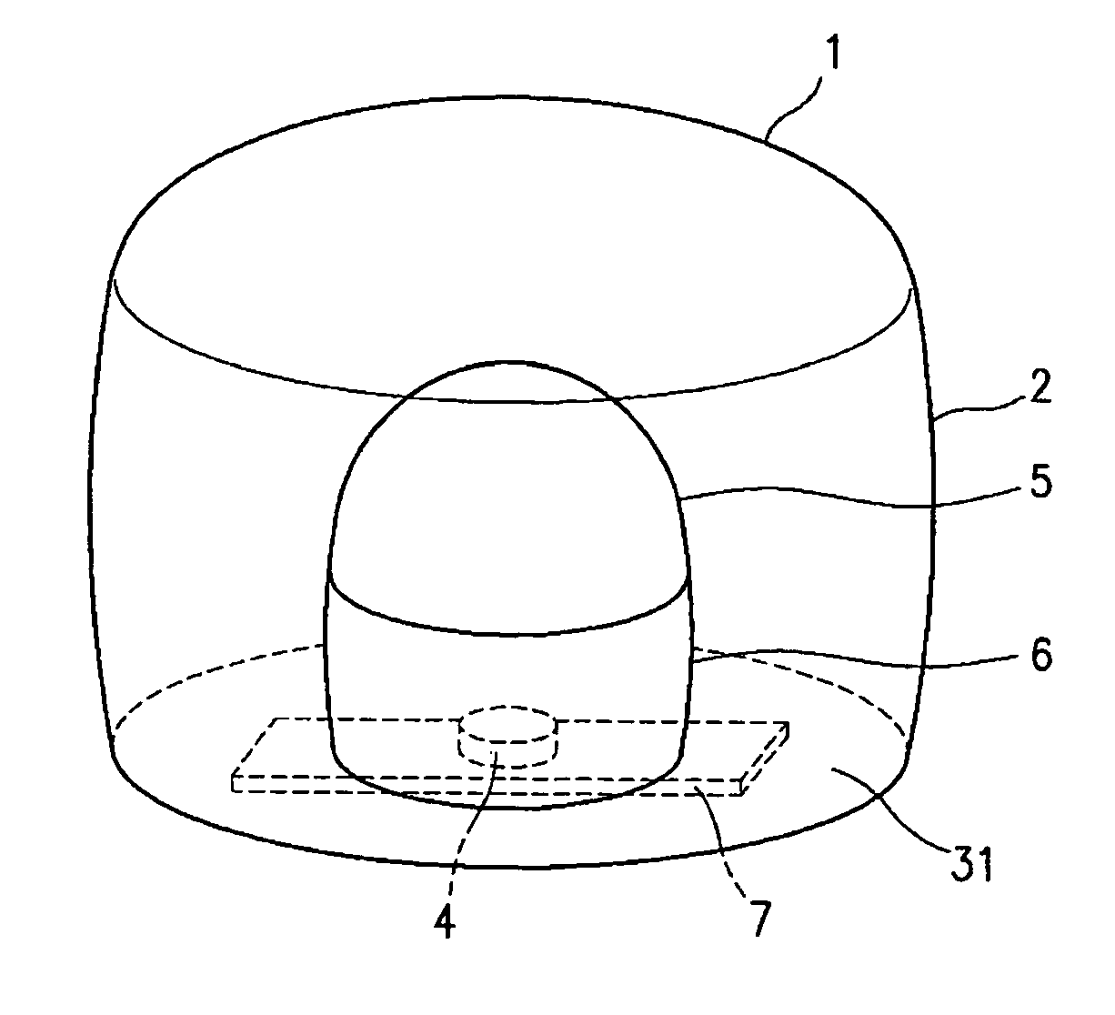
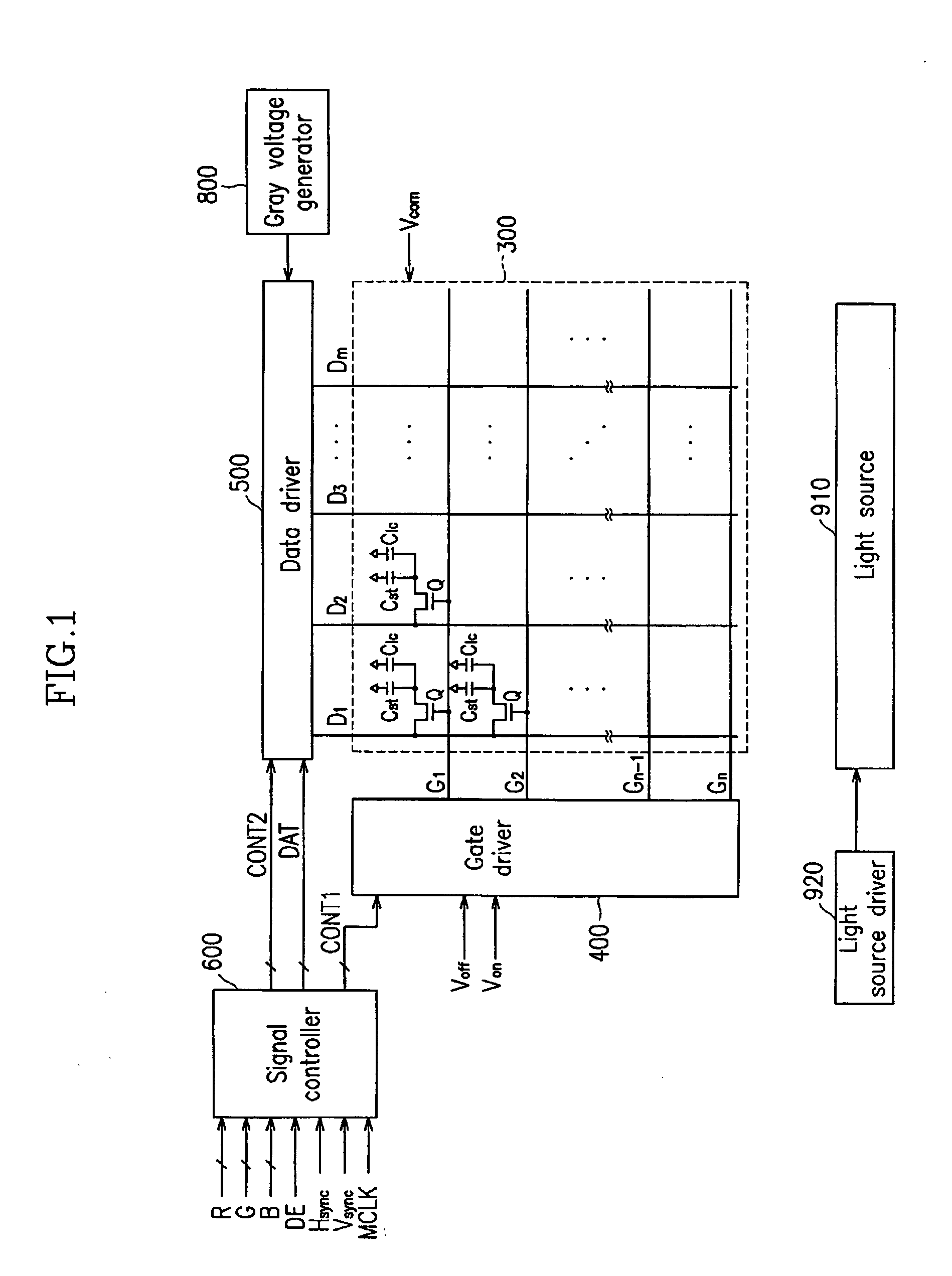
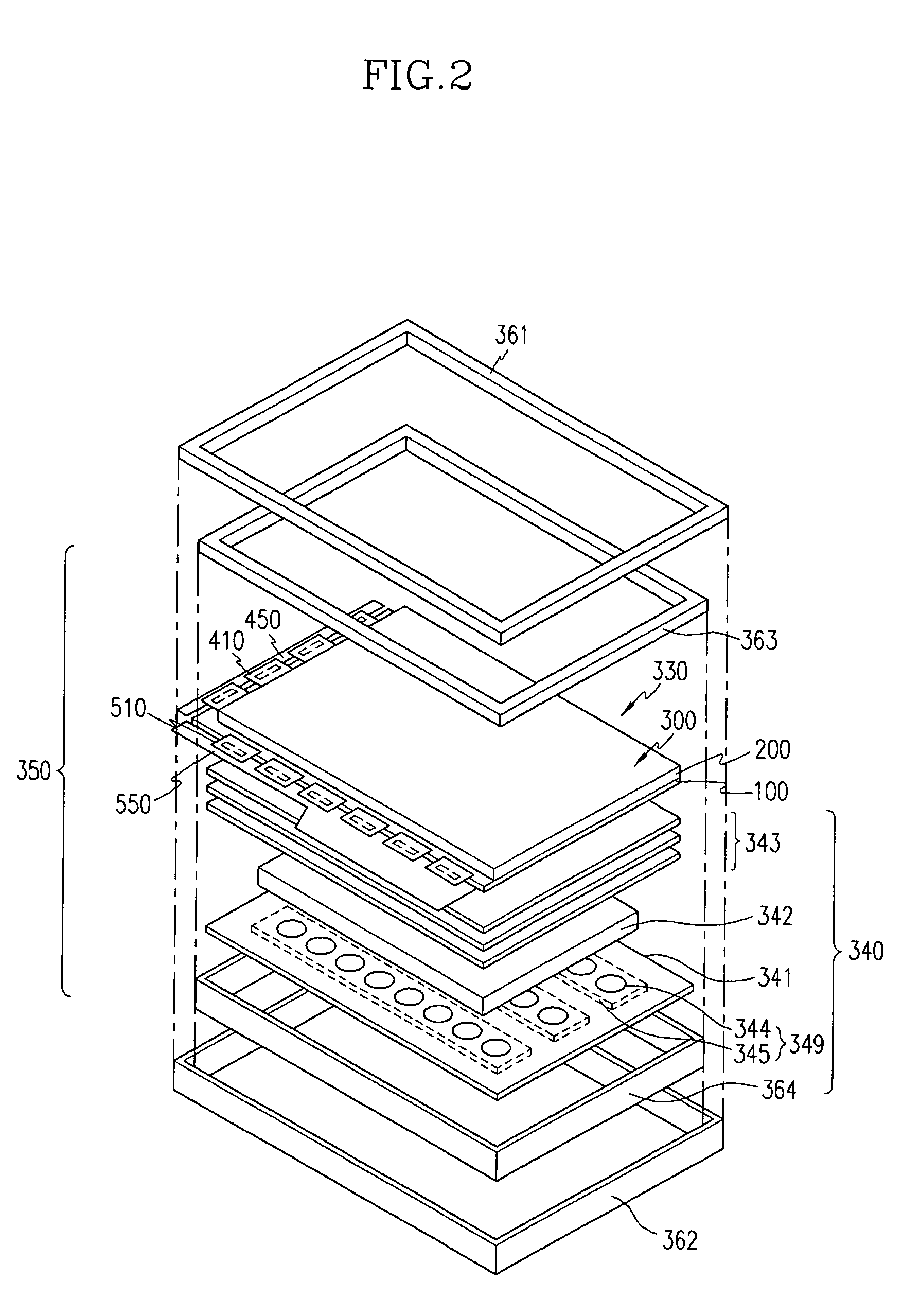
[0092] Hereinafter, a light source device for a display device according to preferred embodiments of the ...


PUM


Abstract

A lens for a light emitting diode is formed with a material having a refractive index of n, and the lens includes a base, a first curved circumferential surface extending from the base, a curved center-edge surface extending from the first curved circumferential surface, and a curved centermost surface extending from the curved center-edge surface. The base includes a groove for receiving a light emitting chip therein. In the lens, a distance from a center of the base to a point of the curved center-edge surface is always shorter than the radius of curvature for the point of the curved center-edge surface. The curved centermost surface has a concave shape with respect to the base. In addition, when an obtuse angle formed between a main axis of the lens and a tangent line of a point of the curved centermost surface is A1, and an acute angle formed between a straight line linking the center of the base to the point of the curved centermost surface and the main axis of the lens is A2, the lens satisfies the equation: A1+A2<90+sin−1(1/n).

Description

BACKGROUND OF THE INVENTION [0001] (a) Technical Field [0002] The present disclosure relates to a light source for a display device. [0003] (b) Discussion of the Related Art [0004] Display devices used for image display such as in a television receiver or computer monitor are classified into a self-luminescence display and a light-receiving display requiring a separate light source. Light emitting diode (LED), electroluminescence (EL), vacuum fluorescent display (VFD), field emission display (FED), and plasma display panel (PDP) devices, etc., are included in the self-luminescence display device, while liquid crystal displays (LCDs), etc., are included in the light-receiving display devices. [0005] The LCD includes, for example, a pair of panels individually having electrodes on their inner surfaces, and a dielectric anisotropy liquid crystal layer interposed between the panels. In the LCD, a variation of the voltage difference between the field generating electrodes, i.e., the vari...

Claims


Application Information

Patent Timeline
Patent Type & Authority Applications(United States)
IPC IPC(8): F21V3/00F21V5/00H01L33/58
CPCF21V5/04F21Y2101/02G02B3/04H01L33/54H01L33/58F21V5/008G02F1/133603G02B19/0014G02B19/0061F21Y2115/10G02F1/1335
Inventor YOON, JU-YOUNGKIM, GI-CHERLLEE, JONG-SEOSONG, CHUN-HOPARK, SE-KILEE, SANG-GILKANG, SEOCK-HWAN
Owner SAMSUNG DISPLAY CO LTD
Why Eureka
Try Eureka