Nonvolatile semiconductor memory

a semiconductor memory and non-volatile technology, applied in static storage, digital storage, instruments, etc., can solve the problems of potential generating circuits operating continuously, increasing production costs, and deteriorating reading margins, so as to reduce production costs and reduce unstable factors

Active Publication Date: 2006-04-20
PANASONIC SEMICON SOLUTIONS CO LTD
View PDF8 Cites 42 Cited by
  • Summary
  • Abstract
  • Description
  • Claims
  • Application Information

AI Technical Summary

Benefits of technology

[0026] It is an object of the present invention to provide a nonvolatile semiconductor device capable of suppressing unstable factors caused due to variation in the power supply characteristic of the circuit or the temperature characteristic of the memory c

Problems solved by technology

However, according to the reading system using the transistor having the structure completely identical to the memory cell transistor as the reference cell transistor, such problems existed that, because a write level of the reference cell transistor must be set prior to the product delivery, a production cost is increased and that, because the reference cell current is varied when a quantity of charge in the floating gate of the reference cell transistor is varied due to the external stress, the temperature stress, or the like in the reading operation, a reading margin is deteriorated.
Alternately,

Method used


Image

  • Nonvolatile semiconductor memory
  • Nonvolatile semiconductor memory
  • Nonvolatile semiconductor memory

Examples


embodiment 1

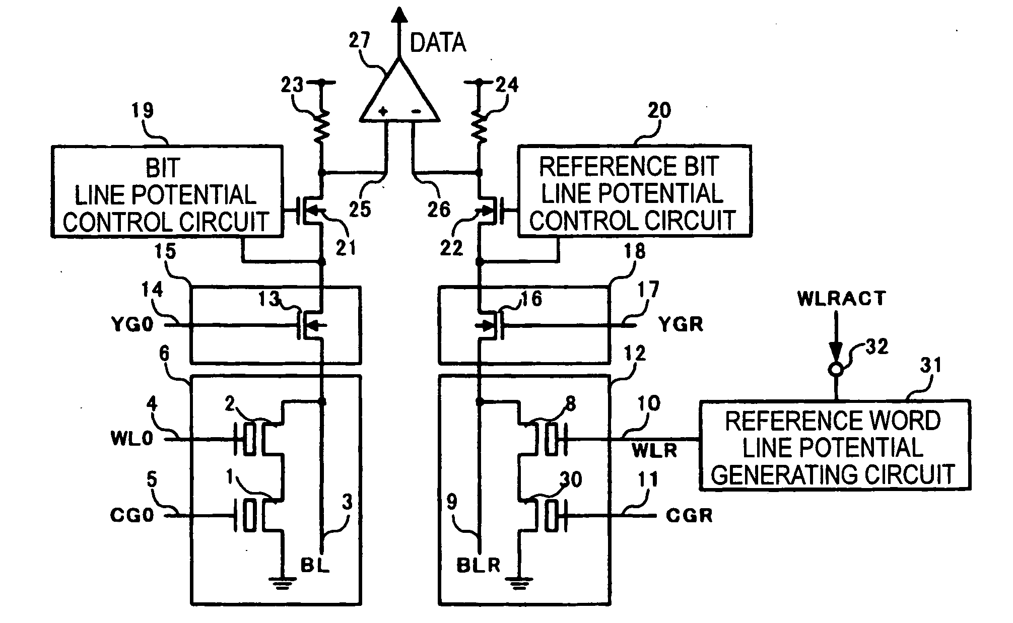
[0074]FIG. 1 is a block diagram showing an overall configuration of a nonvolatile semiconductor device according to an embodiment 1 of the present invention. In FIG. 1, 1 is the memory cell transistor, 2 the memory cell selecting transistor, 3 the bit line, 4 the word line, 5 the memory cell transistor control gate line, 6 the memory cell array composed of nonvolatile memory cells, 8 the reference cell selecting transistor, 9 the reference bit line, 10 the reference word line, 11 the reference cell transistor control gate line, and 12 the reference cell array composed of reference cells.

[0075] Also, 13 is the column gate, 14 the column gate selecting line, 15 the column decoder, 16 the reference column gate, 17 the reference column gate selecting line, 18 the reference column decoder, 19 the bit line potential control circuit, 20 the reference bit line potential control circuit, 21 the bit line potential control transistor, 22 the reference bit line potential control transistor, 23...

embodiment 2

[0096]FIG. 5 and FIG. 6 are a circuit diagram showing a configuration of the reference word line potential generating circuit of the nonvolatile semiconductor memory according to an embodiment 2 of the present invention respectively. Also, FIG. 7 is a waveform diagram explaining an operation of the present embodiment. An overall configuration of the nonvolatile semiconductor memory is similar to that in FIG. 1 explained in the embodiment 1.

[0097] In FIG. 5, 60 is a reference word line driver, 61, 62 potential generating means, 63 an output node from the potential generating means 61, 62, 64 a signal READ activated in a reading operation mode period, 65 a signal ACT1 for activating the word line potential generating means 61, 66 a signal ACT2 for activating the word line potential generating means 62, and 67 a delayed pulse generating means.

[0098] In the nonvolatile semiconductor memory constructed as above, the signal READ is activated in the reading mode. Then, when WLRACT of the...

embodiment 3

[0108]FIG. 8 is a circuit diagram showing a configuration of the reference word line potential generating circuit of a nonvolatile semiconductor memory according to an embodiment 3 of the present invention. FIG. 9 is a waveform diagram explaining an operation of the present embodiment. An overall configuration of the nonvolatile semiconductor memory is similar to that in FIG. 1 explained in the embodiment 1.

[0109] In FIG. 8, 60 to 66 are constituent elements of the reference word line potential generating circuit similar to those shown in FIG. 5, and 70 is a smoothing capacitor that makes the potential of the output node 63 smooth when the signal WLRACT is activated to supply the current.

[0110] Here, the current supply capability and the consumption current of the potential generating means 62 are set smaller than those of the potential generating means 61. The potential generating means 61 is activated only by WLRACT of the reference cell selecting signal 32, while the potential ...


PUM


Abstract

A nonvolatile semiconductor memory includes a memory cell 6 composed of a memory cell transistor 1 having a floating gate and a control gate and a memory cell selecting transistor 2, a reference cell 12 composed of a reference cell transistor 30 having the same structure as the memory cell transistor 1 and a reference cell selecting transistor 8, and a reference word line potential generating circuit 31 connected to a gate of the reference cell selecting transistor 8, wherein, in a reading operation, the same power supply voltage is applied between a floating gate and a source node of the reference cell transistor 30, and an intermediate potential between a potential applied when the memory cell selecting transistor 2 is selected and a potential applied when the memory cell selecting transistor 2 is not selected is applied to the gate of the reference cell selecting transistor 8.

Description

BACKGRUOD OF THE INVENTION [0001] 1. Field of the Invention [0002] The present invention relates to a nonvolatile semiconductor memory capable of reading stably data at a high speed by using a differential sense amplifier that compares / decides a memory cell current and a reference cell current. [0003] 2. Description of the Related Art [0004] In the nonvolatile semiconductor memory such as the flash type, EEPROM, or the like, a charge injection into a floating gate of the memory cell transistor and a charge extraction from there is executed by a writing operation, then a difference in a quantity of charge held in the floating gate is sensed as a memory cell current, and then this current is read as data. [0005] In the flash type nonvolatile semiconductor memory, in order to realize a stable reading operation by maintaining a constant amount of memory cell current over a wide power supply voltage range in the time of reading, a measure is taken to set control gate potential applied to...

Claims


Application Information

Patent Timeline
IPC IPC(8): G11C16/06
CPCG11C16/04G11C16/28G11C16/30G11C29/02G11C29/021G11C29/028
Inventor ARAKAWA, KEN
Owner PANASONIC SEMICON SOLUTIONS CO LTD
Why Eureka
Try Eureka