Unlock instant, AI-driven research and patent intelligence for your innovation.

Method for optimizing integrated circuit device design and service

a technology of integrated circuit devices and optimization methods, applied in the direction of cad circuit design, program control, instruments, etc., can solve the problems of large intermediate bdd sizes, difficult to find good hints, and difficult to identify good hints, etc., to facilitate improved analysis of integrated circuit device design

Inactive Publication Date: 2006-04-20
GLOBALFOUNDRIES INC
View PDF3 Cites 21 Cited by
  • Summary
  • Abstract
  • Description
  • Claims
  • Application Information

AI Technical Summary

Benefits of technology

[0007] Having in mind the field and problems identified above, one purpose of this invention is to facilitate improved analysis of integrated circuit device design. In realizing this purpose of this invention, the state explosion problem is preempted by constructing systems small enough to make automatic checking tractable, yet large enough to capture the information relevant to the property being checked—reachability in this case. The method here disclosed exploits these ob

Problems solved by technology

One problem encountered in such analysis is referred to as a “state explosion”, which occurs when an input to the design, intended to permit analysis of the response of the device to a particular input, generates such a large number of possible output or intermediate states as to overrun any memory used in supporting the analysis.
However, the known state explosion problem may cause large intermediate BDD sizes during the exploration of the state space of a system.
However, the ease of finding good hints is limited by the size and complexity of the design, and extending their applicability to larger designs is a key issue.
However, in large complex designs, identifying good hints can be a labor-intensive process requiring many attempts, and in most cases does not avoid the state space explosion problem.

Method used


Image

  • Method for optimizing integrated circuit device design and service
  • Method for optimizing integrated circuit device design and service
  • Method for optimizing integrated circuit device design and service

Examples


Embodiment Construction

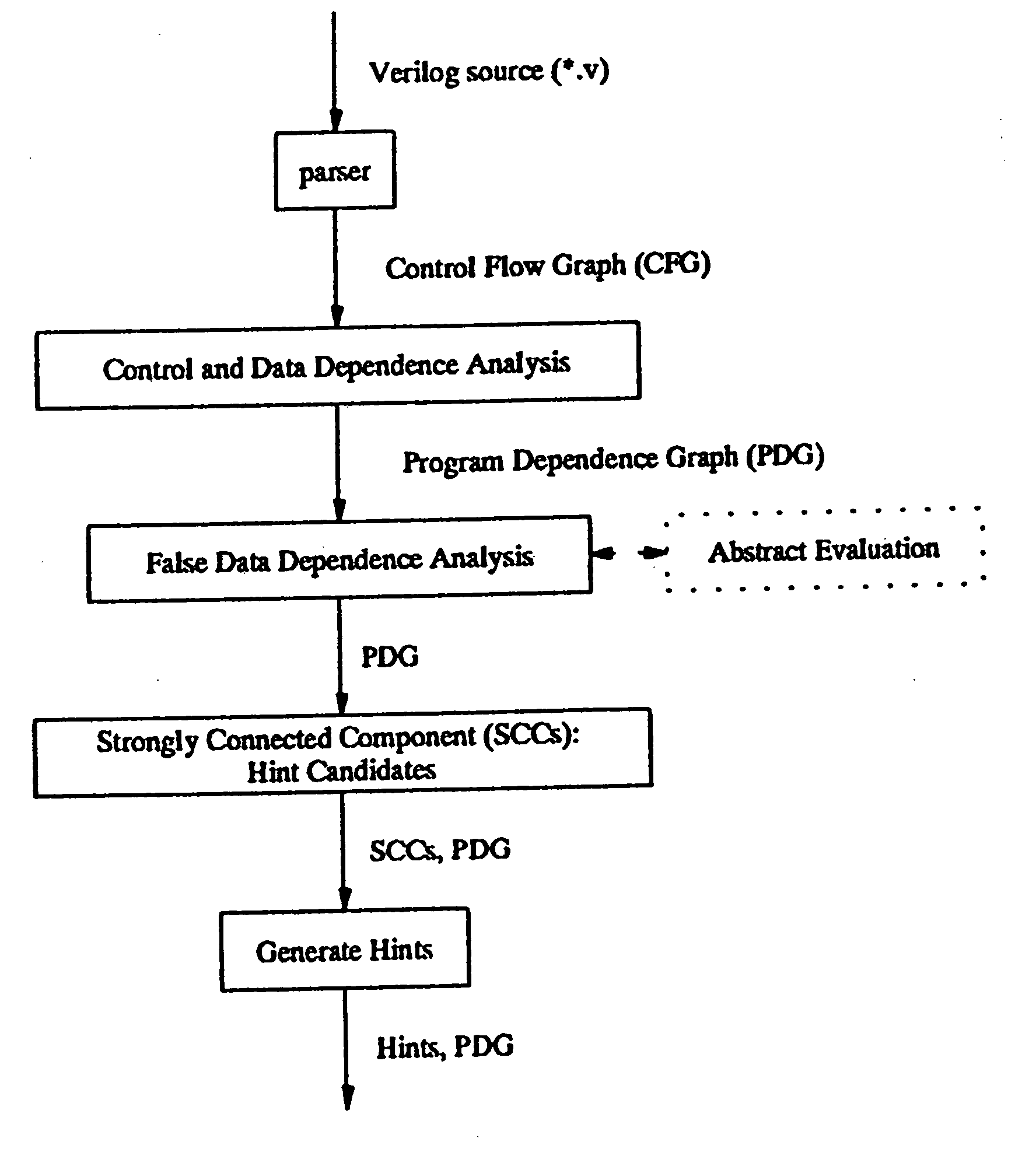
[0011] While the present invention will be described more fully hereinafter with reference to the accompanying drawings, in which a preferred embodiment of the present invention is shown, it is to be understood at the outset of the description which follows that persons of skill in the appropriate arts may modify the invention here described while still achieving the favorable results of the invention. Accordingly, the description which follows is to be understood as being a broad, teaching disclosure directed to persons of skill in the appropriate arts, and not as limiting upon the present invention. In particular, while the context for this disclosure is the design of integrated circuit devices, it is known that the “state explosion” problem here addressed is also found in software design and believed that the techniques and method here described will find usefulness in such applicatins.

[0012] The program analysis techniques employed to accomplish the objective outlined above are...


PUM


Abstract

Improved analysis and refinement of integrated circuit device design and other programs is facilitated by methods in which an original program is partitioned into subprograms representing valid computational paths; each subprogram is refined when cyclic dependencies are found to exist between the variables; computational paths whose over-approximated reachable states are found to be contained in another computational path are merged; and finally, the remaining subprograms conjoined decision conditions become candidates for hints for program refinement.

Description

FIELD AND BACKGROUND OF INVENTION [0001] This invention relates to integrated circuit design techniques. [0002] The design of integrated circuit devices conventionally uses hardware description languages (HDLs) to describe circuits (herein also sometimes called “systems”) at various levels of abstraction. As a circuit design evolves, designers and verification engineers (whose job it is to assure that the design functions appropriately) conduct analysis of the device being designed to evaluate the quality of the design and to hopefully find and eliminate any inadequacies potentially leading to future problems such as impossibility or inaccuracy in performance of the device. [0003] One problem encountered in such analysis is referred to as a “state explosion”, which occurs when an input to the design, intended to permit analysis of the response of the device to a particular input, generates such a large number of possible output or intermediate states as to overrun any memory used in...

Claims


Application Information

Patent Timeline
IPC IPC(8): G06F17/50G06F9/45
CPCG06F17/5045G06F30/30
Inventor WARD, DAVID
Owner GLOBALFOUNDRIES INC