
Package structure for optical-electrical semiconductor

Inactive Publication Date: 2006-04-27
HARVATEK CORPORATION
View PDF12 Cites 18 Cited by
  • Summary
  • Abstract
  • Description
  • Claims
  • Application Information

AI Technical Summary

Benefits of technology

[0007] The major purpose of present invention is to provide a package structure with simple structure with high-quality light focusing for an optical-electrical semiconductor, and particularly for LEDs, that is suitable for cheap, high quality mass production.
[0008] To achieve the above purpose, the present invention discloses a packaging structure that is formed in one piece as shell with a chip-receiving device (without the cup wall for light reflection) and further uses heat-conducting material for heat dissipation. The present invention also is easy to manufacture on conventional packaging machines.

Problems solved by technology

Further, the brightness of an LED is a very important issue for the LED package.
The conventional assembly procedure suffers from drawbacks, and the cup wall (surrounding the cup surface 40a) reflects light (like the reflection cup of a electric flashlight) without focusing to a point.
Further, the base 50a is not integral with the embedded injection body 10a and is expensive to assemble.

Method used


Image

  • Package structure for optical-electrical semiconductor
  • Package structure for optical-electrical semiconductor
  • Package structure for optical-electrical semiconductor

Examples


Embodiment Construction

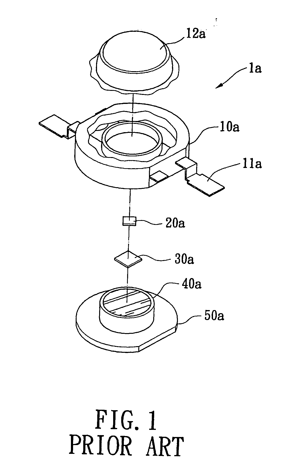
[0022] The basic principle of the invention is use a lens to focus light to a point (or a local region) to raise the quality of light radiation and remove an unnecessary component (such as the cup wall for light reflection in the prior art). The present invention is especially applicable to situation where high quality light (or image) must be focused on a local area (such as scanner or digital camera). In addition, the present invention uses a shell body integrally formed in one piece for a good heat conduction effect and ease of assembly.

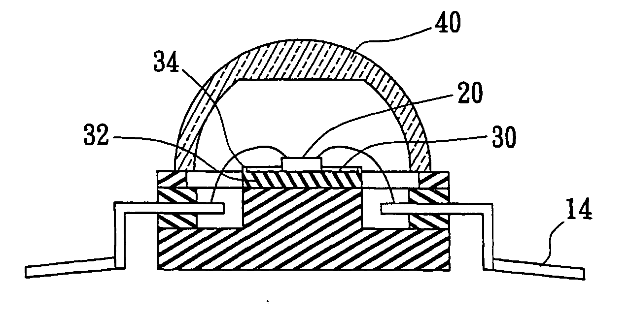
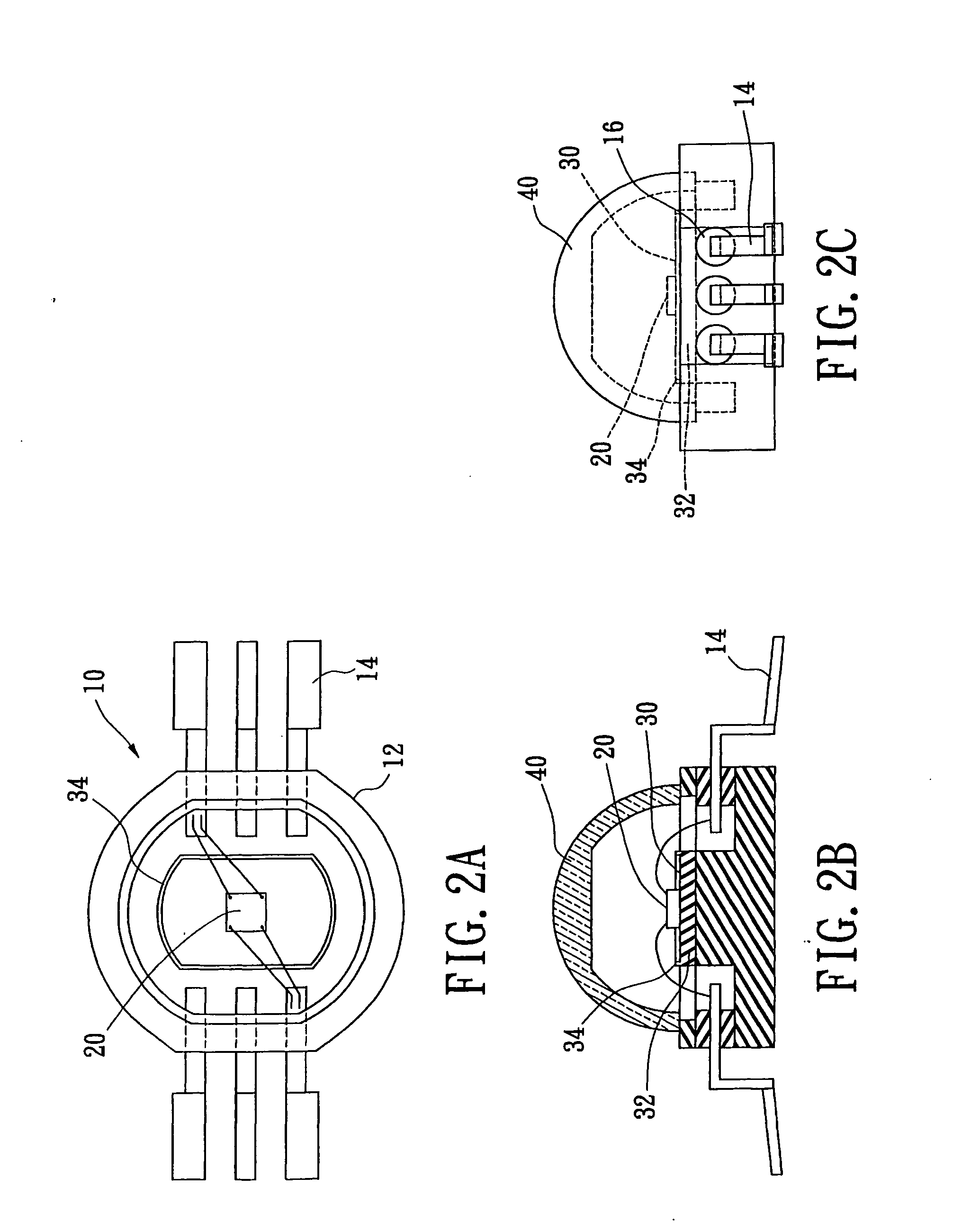
[0023] In addition, the present invention also can use wire bonding as a packaging method, as illustrated in FIG. 2A and FIG. 2B. The present invention also can use an optical-electrical product having an outer transparent polymer coating (like a SMT product).

[0024] Reference is made to FIGS. 2A to 2C, 3A to 3C and 4A to 4C. Package structures of an optical-electrical semiconductor for the present invention are illustrated therein. The present i...


PUM


Abstract

A package structure for an optical-electrical semiconductor is described. The package structure has a thermal conductive structure for heat transfer and is integrally formed in one piece to improve the structural strength thereof, while the thermal conductive structure prevent over-heating of the LED device for greater longevity. The package structure reduces the failure rate in production and has improved quality. When the present invention is applied in light-emitting diode packages, the special requirement can be reached and has better properties than the prior art.

Description

BACKGROUND OF THE INVENTION [0001] 1. Field of the Invention [0002] The present invention relates to a package structure for an optical-electrical semiconductor. The benefit of the present invention is that the thermal conductive structure for heat transfer is integrally formed in one body. The effect of the present invention can reduce the failure rate of production, improve the quality thereof, and decrease structural deformation. When the present invention is applied in a light-emitting diode package, the special requirement can be reached and has better properties than the prior art. The main feature of the present invention is integral formation in one structure to improve the structural strength with a thermal conductive structure to prevent overheating of the LED device for long use and avoiding waste in the assembly procedure. [0003] 2. Description of Related Art [0004] In the industry of chip packaging, one special object for a skilled person is a package for an optical-ele...

Claims


Application Information

Patent Timeline
IPC IPC(8): H01L33/00H01L33/48H01L33/58H01L33/64
CPCH01L25/0753H01L31/0203H01L33/486H01L33/58H01L33/642H01L2224/49113H01L2224/48091H01L2224/48247H01L2924/00014
Inventor WANG, BILYCHUANG, JONNIEWU, SHIH-YUKO, CHING-HUNGWENG, CHUN-CHENG
Owner HARVATEK CORPORATION
Learn More