X-ray thin film inspection apparatus and thin film inspection apparatus and method for patterned wafer

a thin film inspection and inspection apparatus technology, applied in the direction of instruments, radiation beam directing means, semiconductor/solid-state device testing/measurement, etc., can solve the problem of large cost load on semiconductor device makers' inspection wafers, low measurement precision of thin films of several nm, etc., to achieve the effect of sufficient precision

Active Publication Date: 2006-04-27
RIGAKU CORP
View PDF12 Cites 47 Cited by
  • Summary
  • Abstract
  • Description
  • Claims
  • Application Information

AI Technical Summary

Benefits of technology

[0027] According to the present invention, there can be provided the X-ray thin film inspection apparatus that can be installed in the manufacturing process of film-formed products and with which direct inspection can be carried out on the products themselves and even thin film of several nm level in thickness can be examined with sufficient precision without throwing away a wafer after inspection.

Problems solved by technology

Furthermore, the film thickness inspection apparatus using optical interference or ellipsometry and the opto-acoustic type apparatus are suitable for the in-line process, however, the measurement precision thereof is too low to measure the thin film of several nm.
Wafers for inspection (blanket wafers) which are used once for inspection and then thrown away are a large cost load for semiconductor device makers.
Particularly, the diameter of semiconductor wafers has been increased, and the cost needed for one blanket wafer has been also increased.

Method used


Image

  • X-ray thin film inspection apparatus and thin film inspection apparatus and method for patterned wafer
  • X-ray thin film inspection apparatus and thin film inspection apparatus and method for patterned wafer
  • X-ray thin film inspection apparatus and thin film inspection apparatus and method for patterned wafer

Examples


Embodiment Construction

[0050] Preferred embodiments according to the present invention will be described hereunder in detail with reference to the accompanying drawings when the present invention is applied to thin film inspection of a semiconductor wafer.

[0051] It is needless to say that the present invention is not limited to thin film inspection of semiconductor wafers, but it may be applied to thin film inspection of various kinds of devices having a multilayer film structure achieved by laminating many thin films on a substrate. Construction of X-ray Thin Film Inspection Apparatus:

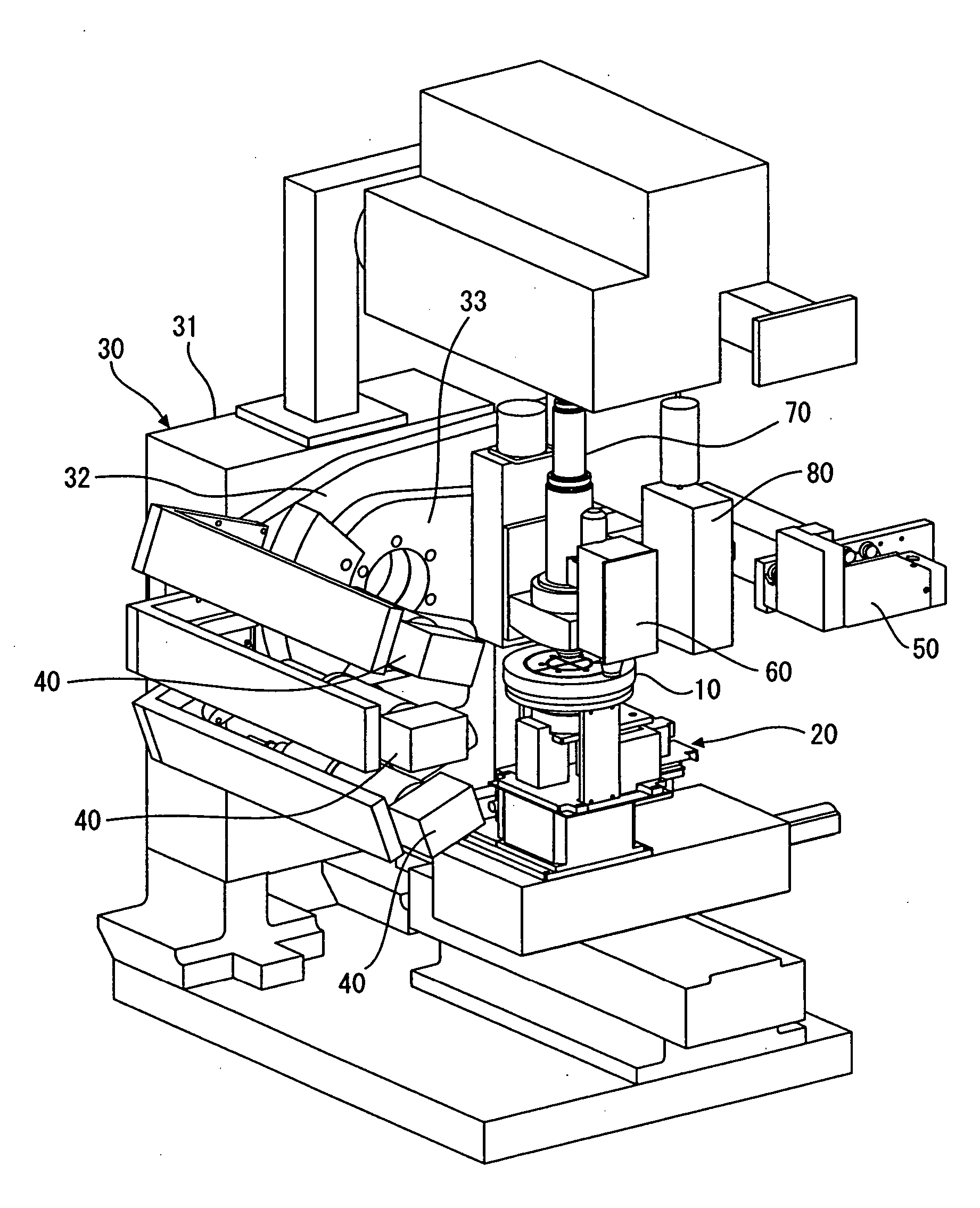
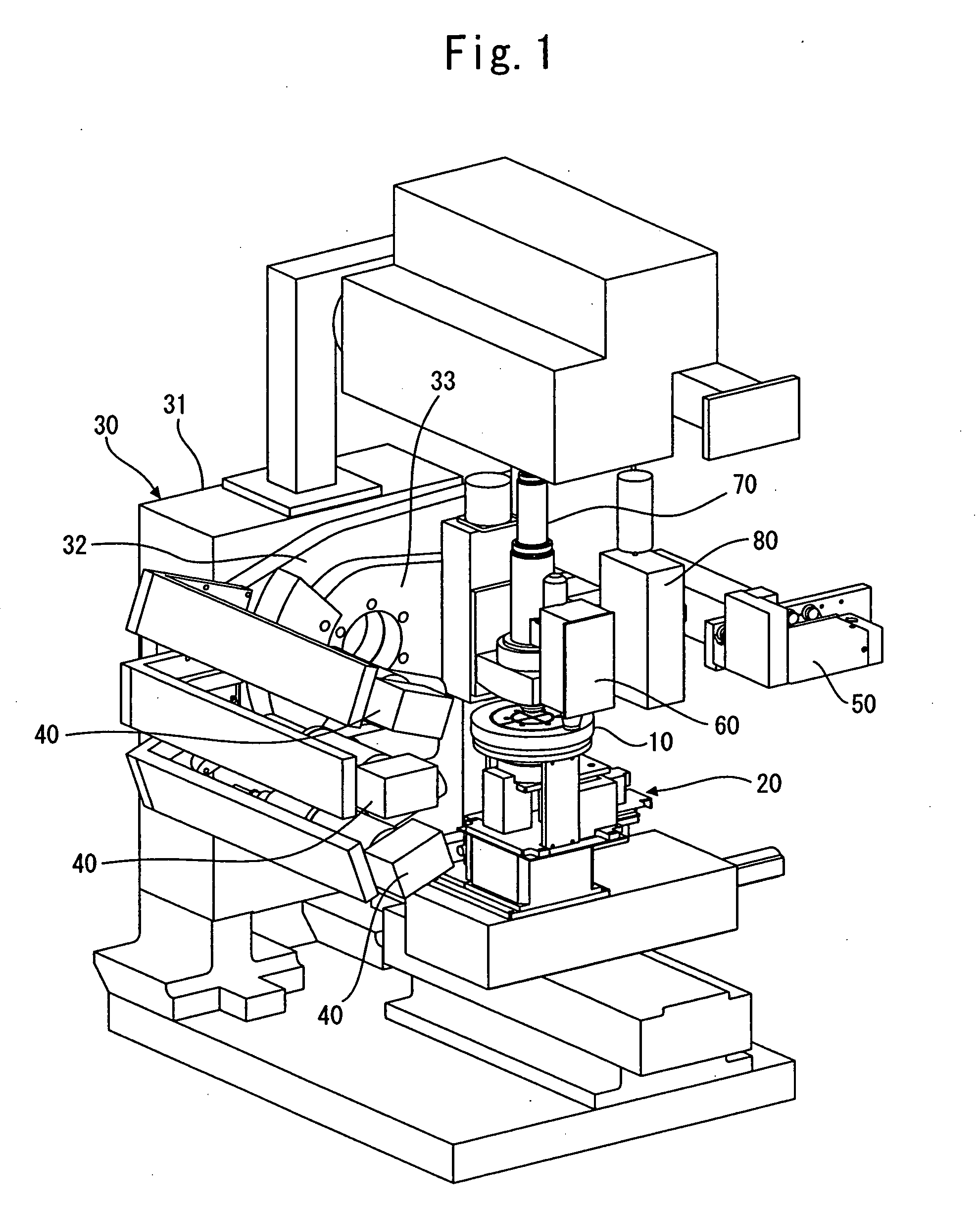
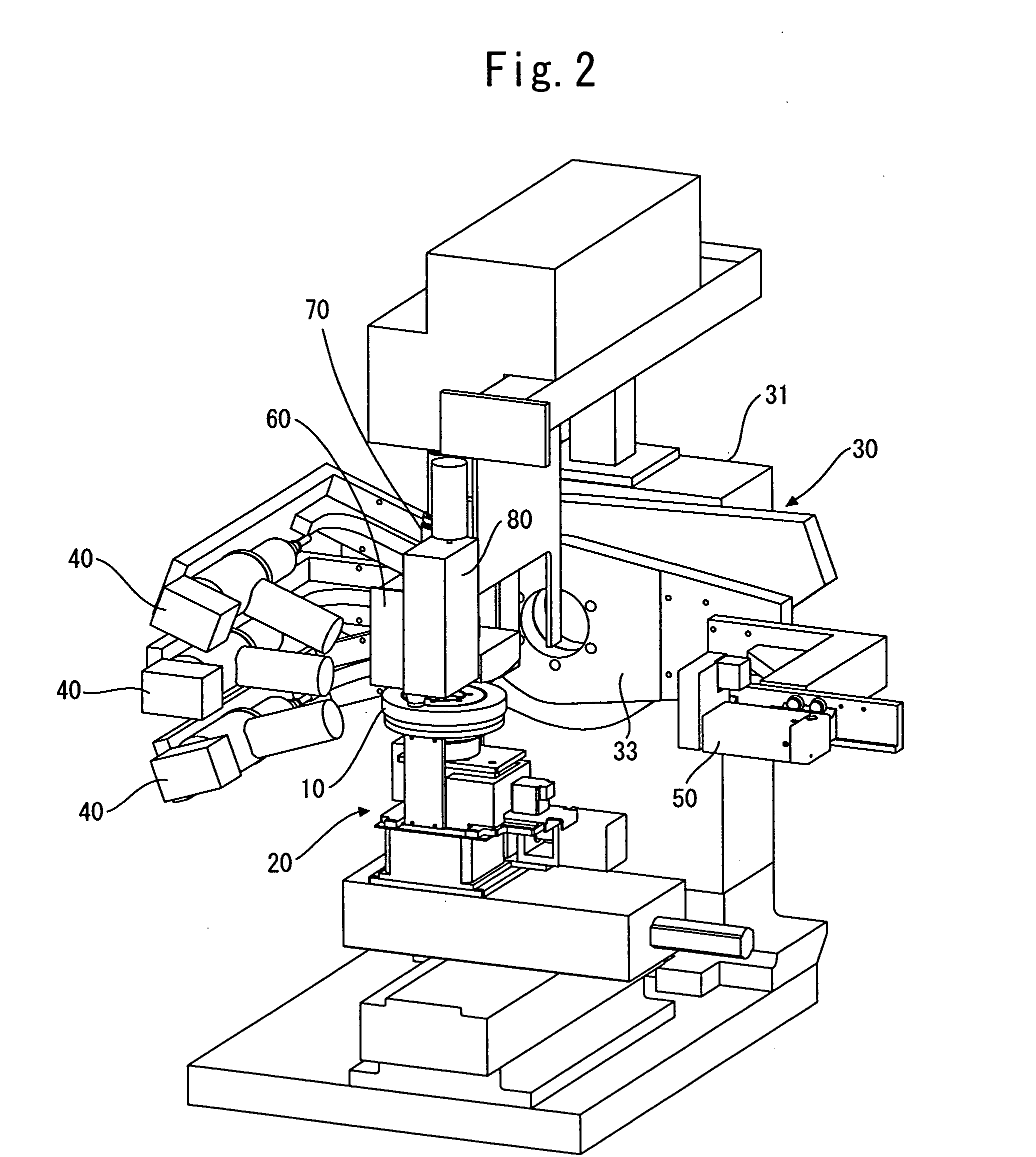
[0052]FIGS. 1 and 2 are perspective views achieved when the overall structure of the X-ray thin film inspection apparatus according to the embodiment is viewed from different visual fields, and FIG. 3 is a front view showing the X-ray thin film inspection apparatus.

[0053] The X-ray thin film inspection apparatus is equipped with a sample table 10, a positioning mechanism 20, a goniometer 30, an X-ray irradiation unit 40,...


PUM

PropertyMeasurementUnit
diameteraaaaaaaaaa
aaaaaaaaaa
divergence angleaaaaaaaaaa

Abstract

An X-ray thin film inspection apparatus including a sample table on which an inspection target such as a product wafer or the like is mounted, a positioning mechanism for moving the sample table, a goniometer having first and second swing arms, at least one X-ray irradiation unit that are mounted on the first swing arm and containing an X-ray tube and an X-ray optical element in a shield tube, an X-ray detector mounted on a second swing arm, and an optical camera for subjecting the inspection target disposed on the sample table to pattern recognition.

Description

BACKGROUND OF THE INVENTION [0001] 1. Field of the Invention [0002] The present invention relates to an X-ray thin film inspection apparatus suitable for a technical field of manufacturing a device having a multilayer film structure achieved by laminating many thin films on a substrate, such as a semiconductor manufacturing field. [0003] 2. Description of the Related Art [0004] With respect to semiconductor devices or other types of devices in which a multilayer film structure achieved by laminating many thin films is formed on a substrate, the characteristics of these devices are varied in accordance with the film thickness, density, crystallinity, etc. of each thin film to be formed. Recently, the miniaturization and integration of these devices have been advanced, and this tendency has been remarkable. Therefore, a thin film inspection apparatus that can accurately measure the state of each film thus formed has been required. [0005] Direct measurement by a sectional transmission ...

Claims


Application Information

Patent Timeline
Patent Type & Authority Applications(United States)
IPC IPC(8): G01N23/20
CPCG01N23/20016G01N23/20025G01N2223/076G01N2223/1016G01N2223/61G01N23/201G01N23/223G06V10/10H01L22/00
Inventor NAKANO, ASAOKINEFUCHI, TAKAOMOTONO, HIROSHIKIKU, ATSUNORI
Owner RIGAKU CORP
Why Eureka
Try Eureka