Light-emitting display device

a display device and light-emitting technology, applied in the direction of instruments, static indicating devices, etc., can solve the problem of not giving a practical detection method for the above-type variations, and achieve the effect of suppressing effectively the unevenness of the display screen

Inactive Publication Date: 2006-05-04
MATSUSHITA TOSHIBA PICTURE DISPLAY CO LTD
View PDF5 Cites 7 Cited by
  • Summary
  • Abstract
  • Description
  • Claims
  • Application Information

AI Technical Summary

Benefits of technology

[0010] It is an object of the present invention to provide a light-emitting display device able to detect adequately variations in characteristics of light-emitting elements for each pixel and suppressing effectively display unevenness on a screen.
[0015] According to this configuration of the light-emitting display device, emitted light quantity of each pixel, based on the test signal supplied by the test signal supply portion, is detected, and based on this detected value and the test signal, the light-emission characteristic of each pixel is detected, so that variations in the characteristic of the light-emitting element of each pixel are detected adequately, and it is possible to suppress effectively the display unevenness on the screen.

Problems solved by technology

However, International Patent Publication Number WO98 / 40871 does not clearly describe how to set the predetermined reference value when detecting a light-emitting element characteristic.
The driving method described in International Patent Publication Number WO98 / 40871 did not give a practical detection method for the above type of variations in the light-emission characteristics.

Method used


Image

  • Light-emitting display device
  • Light-emitting display device
  • Light-emitting display device

Examples


Embodiment Construction

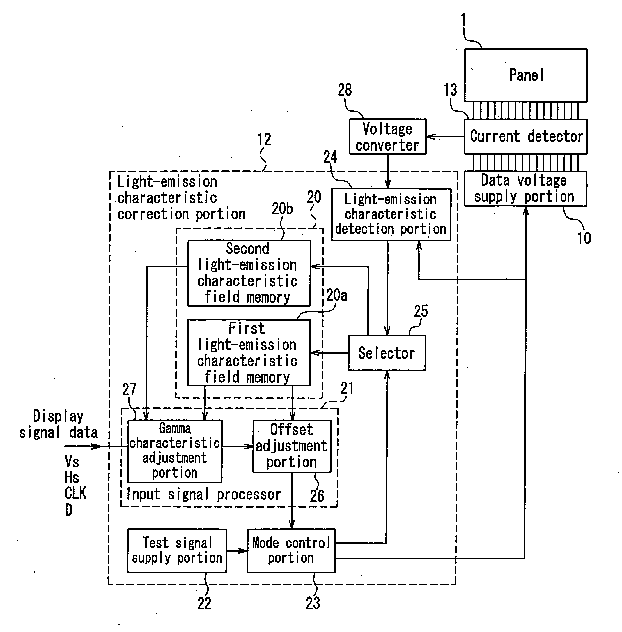
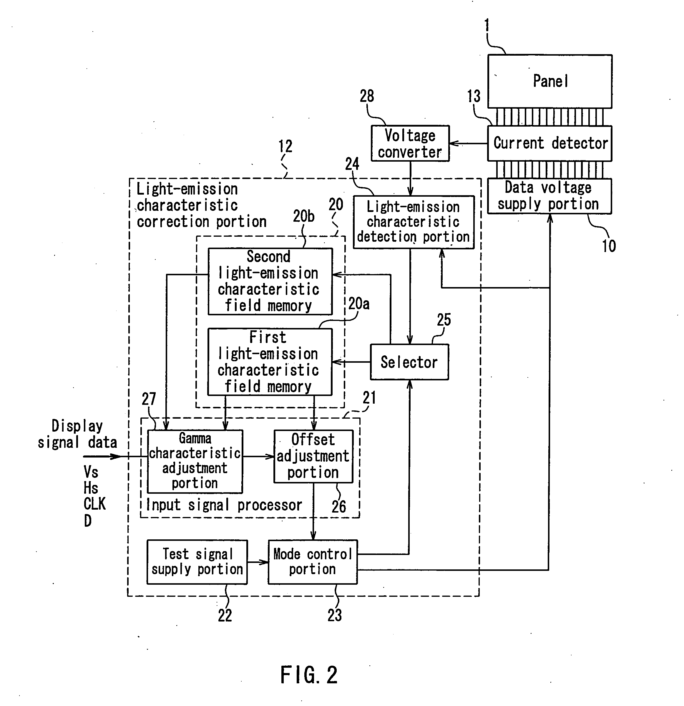
[0021] The light-emitting display device of the present invention having the above-described configuration can be configured so that the light-emission characteristic memory has a first memory for holding first light-emission characteristic data. The display signal processor has an offset adjustment portion that subjects the display signal data to a correction, based on the first light-emission characteristic data of each of the pixels supplied from the first memory, so as to adjust an offset value of the data voltage applied to each of the pixels. The light-emission characteristic detection portion outputs, as the first light-emission characteristic data, the test signal value for each of the pixels at which the output value of the light-emission quantity detector reaches, in the light-emission characteristic detection mode, a first reference value set to have a predetermined relationship with a threshold value of the light-emitting elements.

[0022] In this configuration, the light...


PUM


Abstract

Based on an output signal from a light-emission characteristic correction portion, a data voltage supply portion supplies data voltage to pixels and a light-emission quantity detector detects light-emission quantities of each pixel. The light-emission characteristic correction portion includes a display signal processor for subjecting display signal data to a correction based on a light-emission characteristic held in a memory; a test signal supply portion for generating a test signal in order to apply a test voltage to each pixel; a mode control portion for outputting the output from the display signal processor or the test signal to the data voltage supply portion; and a light-emission characteristic detection portion for detecting the light-emission characteristic of each pixel based on the light-emission quantity detection value and the test signal. The mode control portion performs control so that, in display mode, the output from the display signal processor is supplied to the data voltage supply portion, in light-emission characteristic detection mode, the test signal is supplied to the data voltage supply portion, and output from the light-emission characteristic detection portion is supplied to the memory. Variations in the light-emission characteristic of each pixel can be detected and display unevenness on a screen can be effectively suppressed.

Description

BACKGROUND OF THE INVENTION [0001] 1. Field of the Invention [0002] The present invention relates to light-emitting display devices, for example, inorganic EL (electroluminescent) display devices in which a display panel is composed of inorganic EL elements forming light-emitting elements arrayed as pixels, each pixel being driven selectively to display images. [0003] 2. Description of Related Art [0004] An inorganic EL element has a structure in which a light-emitting layer that includes a phosphor layer and dielectric layers is sandwiched between a pair of electrodes, and emits light when a voltage pulse is applied between the pair of electrodes. A display panel in an inorganic EL display device is configured to have such inorganic EL elements arrayed in a matrix. That is, on a substrate, such as glass, a plurality of stripe electrodes are arranged in parallel with each other, for example in columns, to form data electrodes, and a plurality of stripe electrodes are arranged in par...

Claims


Application Information

Patent Timeline
Patent Type & Authority Applications(United States)
IPC IPC(8): G09G3/10
CPCG09G3/32G09G2300/06G09G2310/0275G09G2320/0233G09G2320/0276G09G2320/0285G09G2320/0295G09G2320/0693
Inventor KATOU, MASAO
Owner MATSUSHITA TOSHIBA PICTURE DISPLAY CO LTD
Why Eureka
Try Eureka