Pattern defect inspecting method, and pattern defect inspecting device

A defect inspection and patterning technology, which is applied in the direction of measuring devices, optical testing flaws/defects, and photo-plate making process on patterned surfaces, etc., can solve problems such as difficulty in inspecting repeated patterns

Inactive Publication Date: 2009-01-07
HOYA CORP
View PDF1 Cites 6 Cited by
  • Summary
  • Abstract
  • Description
  • Claims
  • Application Information

AI Technical Summary

Problems solved by technology

Therefore, when a photomask used in a manufacturing process such as a liquid crystal display device is used as an inspection objec

Method used


Image

  • Pattern defect inspecting method, and pattern defect inspecting device
  • Pattern defect inspecting method, and pattern defect inspecting device
  • Pattern defect inspecting method, and pattern defect inspecting device

Examples


Embodiment Construction

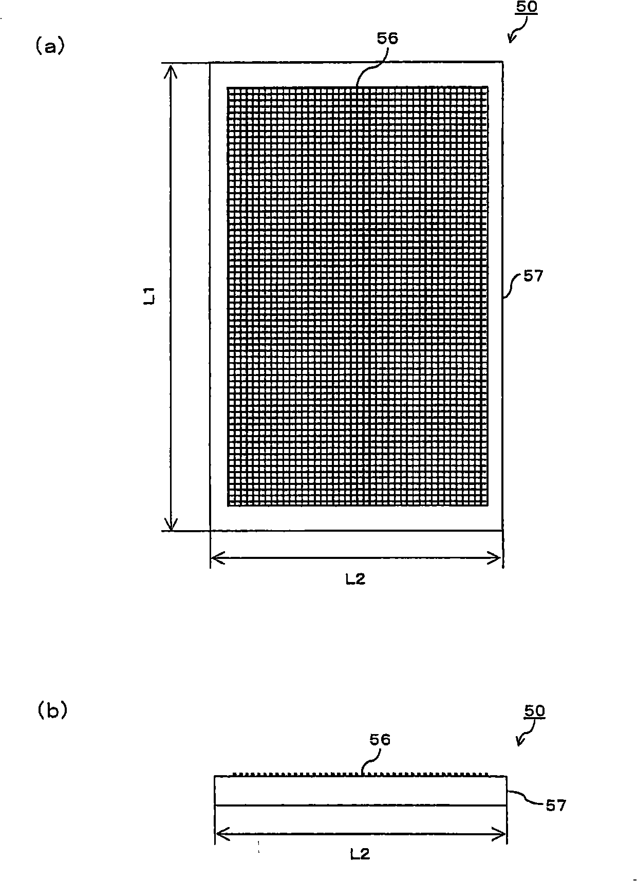
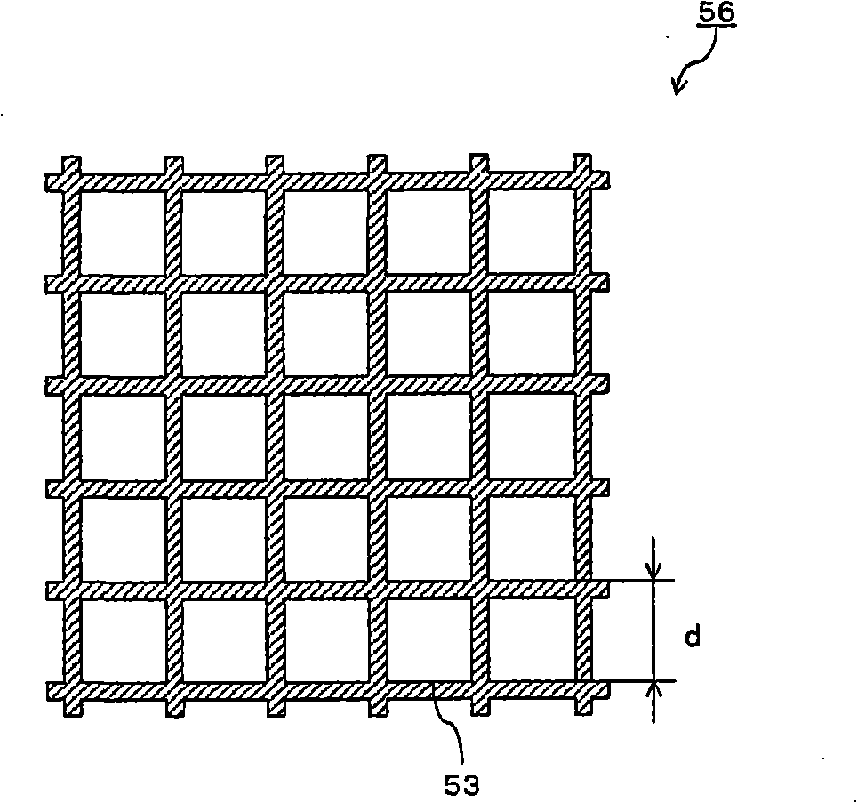
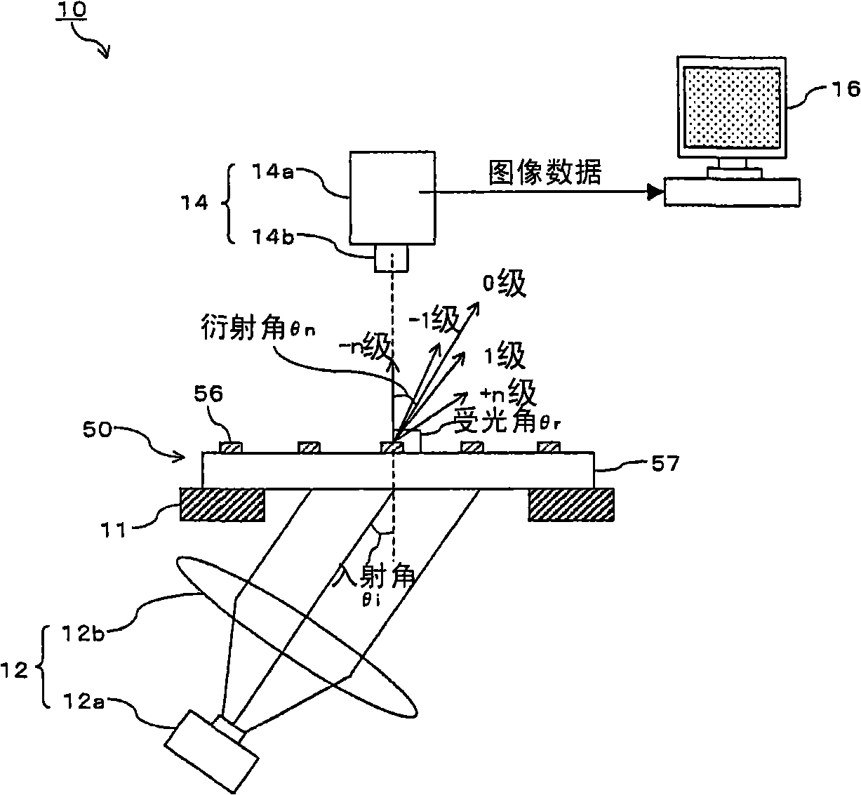
[0036] As described above, Patent Document 1 discloses, for example, using a photomask used in the manufacturing process of a substrate for a semiconductor device having an integrated circuit as an object to be inspected, and inspecting a repetitive pattern generated on the photomask in a short time. method for checking for defects. Here, the problems to be solved by the method disclosed in Patent Document 1 are roughly as follows.

[0037] Conventionally, when the size of a unit pattern of a substrate for a semiconductor device having an integrated circuit is 0.1 μm, it can be checked whether the size variation of the unit pattern is contained within about one-tenth of the size of the unit pattern (that is, about 0.01 μm) within the allowable range. In addition, similarly, when the size of the unit pattern of the photomask used in the manufacturing process of the semiconductor device substrate is 0.4 μm (for example, during the exposure process of 1 / 4), it is also possible t...


PUM

PropertyMeasurementUnit
Spacingaaaaaaaaaa

Abstract

The invention provides a pattern flaw inspection method that inspects the flaw produced in the repeating pattern of an inspection target with the repeating pattern wherein the unit pattern is cyclically arranged. The method has a step of irradiating the repeating pattern with a light at a predetermined incident angle to produce diffracted light; a step of detecting the diffracted light from the repeating pattern to form an image; and a step of observing the image formed by the detection of the diffracted light so as to detect the flaw produced in the repeated pattern. In the step of detecting the diffracted light to make the image form, the ultrahigh order diffracted light of 45th order through 1,600th order in the absolute value for the diffracted light from among the repeating pattern is detected.

Description

technical field [0001] The present invention relates to a pattern defect inspection method and a pattern defect inspection device for inspecting an object to be inspected having a repeated pattern in which unit patterns are periodically arranged, and for defects generated in the repeated pattern. Background technique [0002] For example, on the surface of a display device substrate (Flat Panel Display: FPD) applied to a liquid crystal display device, a plasma display device, an EL display device, an LED display device, a DMD display device, etc., and in the manufacture of the display device substrate A repeating pattern in which unit patterns represented by pixel patterns are periodically arranged is sometimes formed on the surface of the photomask used in the process. The unit patterns are arranged according to a predetermined rule, but due to some reasons in the manufacturing process, for example, some of the unit patterns may contain defects arranged according to a rule ...

Claims


Application Information

Patent Timeline
IPC IPC(8): G03F1/00G01N21/956G01N21/88G03F1/84
CPCG01N21/9501G01N21/95607H01L22/12
Inventor 山口升石川雄大
Owner HOYA CORP
Why Eureka
Try Eureka