Semiconductor device, display device, and electronic device

a technology of semiconductor devices and display devices, applied in semiconductor devices, instruments, computing, etc., can solve the problems of increasing the correction period, difficult to perform external correction in parallel with the display operation of a display device, and unintentional changes of displays, so as to reduce adverse effects, suppress display unevenness, and reduce adverse effects

Inactive Publication Date: 2016-06-02
SEMICON ENERGY LAB CO LTD
View PDF0 Cites 6 Cited by
  • Summary
  • Abstract
  • Description
  • Claims
  • Application Information

AI Technical Summary

Benefits of technology

[0012]An object of one embodiment of the present invention is to provide a display device or the like which can perform external correction in parallel with display operation. An object of one embodiment of the present invention is to provide a driving method of the display device or the like which can perform external correction in parallel with display operation. An object of one embodiment of the present invention is to provide a display device in which display unevenness is suppressed, and a driving method thereof. An object of one embodiment of the present invention is to provide a display device capable of high definition display, and a driving method thereof. An object of one embodiment of the present invention is to provide a semiconductor device which can reduce adverse effects due to variation in transistor characteristics, and a driving method thereof. An object of one embodiment of the present invention is to provide a semiconductor device which can reduce adverse effects due to variation in the threshold voltages of transistors, and a driving method thereof. An object of one embodiment of the present invention is to provide a semiconductor device which can reduce adverse effects due to variation in the motilities of transistors, and a driving method thereof.

Problems solved by technology

Thus, when the external correction is performed while the display operation is performed, display changes unintentionally, in some cases.
For this reason, it is sometimes difficult to perform the external correction in parallel with the display operation of a display device.
Furthermore, in the case where the external correction is performed in a period during which the display operation of the display device is not performed, there has been a problem in that a period for the correction is increased because the correcting operation needs to be performed for a considerable number of pixels.

Method used


Image

  • Semiconductor device, display device, and electronic device
  • Semiconductor device, display device, and electronic device
  • Semiconductor device, display device, and electronic device

Examples


embodiment 1

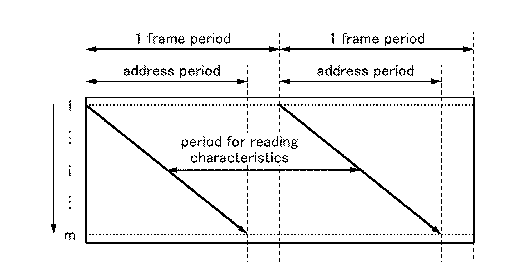
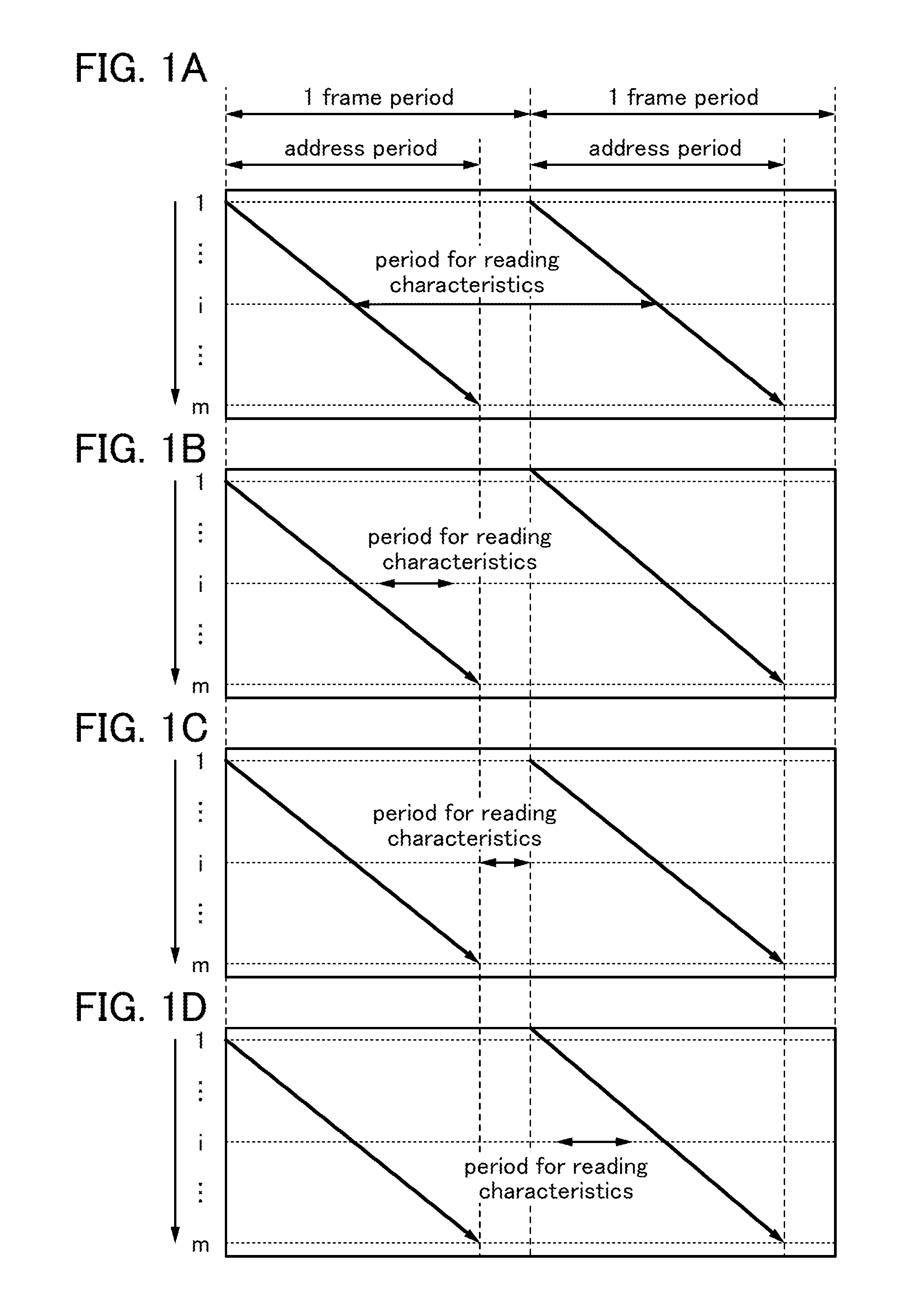
[0081]In this embodiment, a configuration of a semiconductor device according to one embodiment of the disclosed invention and a driving method thereof will be described with reference to FIGS. 1A to 1D to FIGS. 23A and 23B.

[0082]A display device of this embodiment includes a plurality of pixels arranged in a matrix with m rows and n columns (m and n are each an integer greater than or equal to 2). Furthermore, each of the pixels includes a light-emitting element and a transistor which supplies a current to the light-emitting element (hereinafter also referred to as a driving transistor). Furthermore, the display device includes a circuit (also referred to as a reading circuit) which is configured to read out data on current characteristics of the driving transistor to the outside of a pixel portion provided with the pixels. Examples of the data on current characteristics include a current value at the time when a predetermined voltage is supplied to the driving transistor, the thre...

embodiment 2

Example of Variation of Semiconductor Device

[0203]In this embodiment, a structure of a semiconductor device and a driving method thereof which are different from those described in Embodiment 1 are described with reference to FIG. 19 and FIG. 20.

[0204]FIG. 19 shows a pixel structure of the display device of this embodiment. The display device of this embodiment includes, as in the display device in FIG. 3, the pixel portion 15 including (m×n) pixels 70, a variety of peripheral circuits, and a variety of wirings. The same numerals and symbols are used for the peripheral circuits and the wirings.

[0205]FIG. 19 shows a structure of a pixel 70_(i, j) in the i-th row and the j-th column. The pixel 70_(i, j) includes a transistor 71, a p-channel transistor 72, a transistor 73, a light-emitting element 74, and a capacitor 75. Note that these elements included in the pixel 70_(i, j) are connected to the wiring GL_i, the wiring SL_i, the wiring DL_j, the wiring CL_j, and the wiring IL_i.

[0206...

embodiment 3

Structural Example of Pixel

[0217]FIGS. 23A and 23B show layout examples of the pixel that can be used in the above embodiments. Note that the wirings, conductive layers, semiconductor layers, and the like shown by the same hatch pattern in FIGS. 23A and 23B can be formed using the same material in the same process. Although structural examples of the pixel 20 are described here, a similar structure can be applied to the pixel 70.

[0218]The pixel 20 in FIG. 23A includes the transistor 21, the transistor 22, the transistor 23, and the capacitor 25. The pixel also includes a conductive layer 406 having a function of the pixel electrode of the light-emitting element 24. As for connection relations of the elements, the description of FIG. 4 can be referred to. Note that black circles in the drawing represent contact holes.

[0219]The transistor 21 includes a semiconductor layer 411, the transistor 22 includes a semiconductor layer 412, and the transistor 23 includes a semiconductor layer 41...


PUM


Abstract

A display device which can perform external correction in parallel with display operation is provided. The display device includes pixels arranged in a matrix and a reading circuit provided outside the pixels. The pixels each include a light-emitting element and a transistor that supplies a current to the light-emitting element. In this display device, in the case where all of a plurality of specific pixels are displayed in black, variation in current characteristics of a driving transistor is corrected by reading out data on current characteristics of the driving transistor included in a predetermined pixel among the plurality of pixels in an address period.

Description

BACKGROUND OF THE INVENTION[0001]1. Field of the Invention[0002]One embodiment of the present invention relates to a semiconductor device, a display device, an electronic device, a driving method thereof, or a manufacturing method thereof.[0003]Note that one embodiment of the present invention is not limited to the above technical field. The technical field of the invention disclosed in this specification and the like relates to an object, a method, or a manufacturing method. In addition, one embodiment of the present invention relates to a process, a machine, manufacture, or a composition of matter. Specific examples of the technical field of one embodiment of the present invention disclosed in this specification include a light-emitting device, a power storage device, an imaging device, a memory device, a method for driving any of them, and a method for manufacturing any of them.[0004]2. Description of the Related Art[0005]In recent years, display devices have been used for variou...

Claims


Application Information

Patent Timeline
Patent Type & Authority Applications(United States)
IPC IPC(8): G09G3/00
CPCG09G2310/08G09G3/00G09G3/2022G09G3/3208G09G3/3258G09G2300/0408G09G2300/0413G09G2300/043G09G2320/045G09G2360/16G09G2380/02H01L29/78621H01L29/7869H01L29/78696H01L27/1225H10K59/00H10K59/1213
Inventor KIMURA, HAJIME
Owner SEMICON ENERGY LAB CO LTD
Why Eureka
Try Eureka