Semiconductor memory device with on-die termination circuit

a memory device and on-die technology, applied in logic circuit coupling/interface arrangement, pulse technique, instruments, etc., can solve the problems of increasing the sensitivity of signals to external noise, severe reflection, and affecting the effect of effective termination resistance valu

Active Publication Date: 2006-05-04
SK HYNIX INC
View PDF12 Cites 29 Cited by
  • Summary
  • Abstract
  • Description
  • Claims
  • Application Information

AI Technical Summary

Benefits of technology

[0028] It is, therefore, an object of the present invention to provide an on-die termination circuit capable of obtaining a stable effective termination resistance value and stabilizing impedance mism...

Problems solved by technology

However, as the swing widths of signals have been decreased, the signals are more increasingly prone to noises generated from external devices and are severely reflected because of impedance mismatching at an interface terminal.
The impedance mismatching arises due to external noises and various changes in voltage, temperature and process.
The impedance mismatching makes it difficult to transmit data at high speed and causes data outputted from an output terminal to be distorted.
Therefore, when the semiconductor device disposed in the input circuit receives the distorted signal, there may be frequently arising problems of set-up/hold fail and misdetection in an input level.
Meanwhile, in addition to a range of error in an effective termination r...

Method used


Image

  • Semiconductor memory device with on-die termination circuit
  • Semiconductor memory device with on-die termination circuit
  • Semiconductor memory device with on-die termination circuit

Examples


Embodiment Construction

[0039] A semiconductor memory device with an on-die termination circuit in accordance with a preferred embodiment of the present invention will be described in detail with reference to the accompanying drawings.

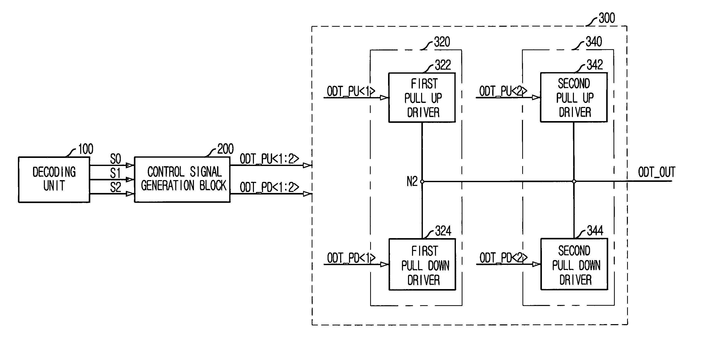
[0040]FIG. 4 is a block diagram showing an on-die termination circuit in a semiconductor memory device in accordance with a preferred embodiment of the present invention.

[0041] As shown, the on-die termination (ODT) circuit includes: a decoding unit 100; a control signal generation block 200; and an ODT output driver block 300. The decoding unit 100 decodes set values of an extended mode register set (EMRS). The ODT output driver block 300 includes a first and a second output driver units 320 and 340 each being connected in parallel with an output node N2 along with a different resistance value. The control signal generation block 200 generates a first and a second pull up control signals ODT_PU and a first and a second pull down control signals ODT_PD for turning on / off th...


PUM


Abstract

An on-die termination circuit with a stable effective termination resistance value and stabilized impedance mismatching. The on-die termination circuit includes: a decoding unit for decoding set values of an extended mode register set; an ODT output driver block including a plurality of output driver units connected in parallel with an output node for outputting an output signal and assigned with different resistance values; and a control signal generation block for generating a plurality of pull up and pull down control signals for turning on/off the plurality of output driver units in response to output signals of the decoding unit.

Description

FIELD OF THE INVENTION [0001] The present invention relates to a semiconductor memory device; and, more particularly, to a semiconductor memory device with an on-die termination circuit capable of obtaining an intended level of termination resistance regardless of changes in process, voltage and temperature. DESCRIPTION OF RELATED ARTS [0002] Various semiconductor devices, for instance, a central processing unit (CPU), a memory, a gate array and so forth, that are implemented as integrated chips are incorporated into electrical products such as personal computers, servers, workstations and the like. In most cases, the semiconductor device includes an input circuit for receiving a variety of signals from an external circuit through input pads and an output circuit for providing internal signals to the external circuit through output pads. [0003] Meanwhile, as operational speed of electrical products is accelerated, swing widths of signals interfaced between the semiconductor devices ...

Claims


Application Information

Patent Timeline
IPC IPC(8): H03K19/003
CPCG11C7/1051G11C7/1057G11C5/063G11C7/22H03K19/017545H04L25/0278
Inventor KIM, YONG-MI
Owner SK HYNIX INC
Why Eureka
Try Eureka