Multi-domain liquid crystal display device and fabrication method thereof

Active Publication Date: 2006-05-04
LG DISPLAY CO LTD
View PDF4 Cites 12 Cited by
  • Summary
  • Abstract
  • Description
  • Claims
  • Application Information

AI Technical Summary

Benefits of technology

[0017] Still another object of the present invention is to provide an LCD device capable of enhancing an ap

Problems solved by technology

Such a disadvantage results from refractive anisotropy of liquid crystal

Method used


Image

  • Multi-domain liquid crystal display device and fabrication method thereof
  • Multi-domain liquid crystal display device and fabrication method thereof
  • Multi-domain liquid crystal display device and fabrication method thereof

Examples


Embodiment Construction

[0037] Reference will now be made in detail to the preferred exemplary embodiments of a multi-domain liquid crystal display (LCD) device and its fabrication method of the present invention, examples of which are illustrated in the accompanying drawings.

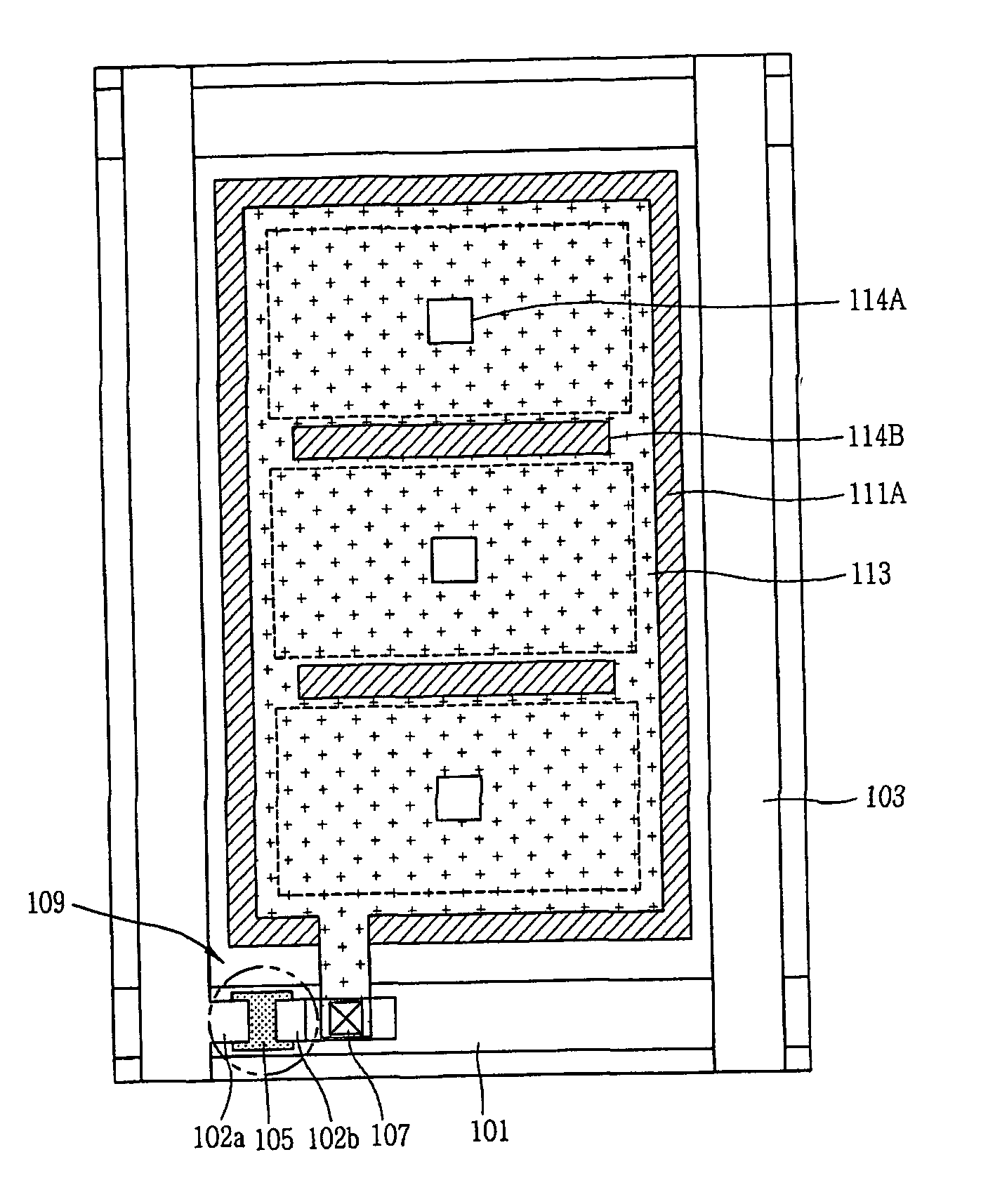
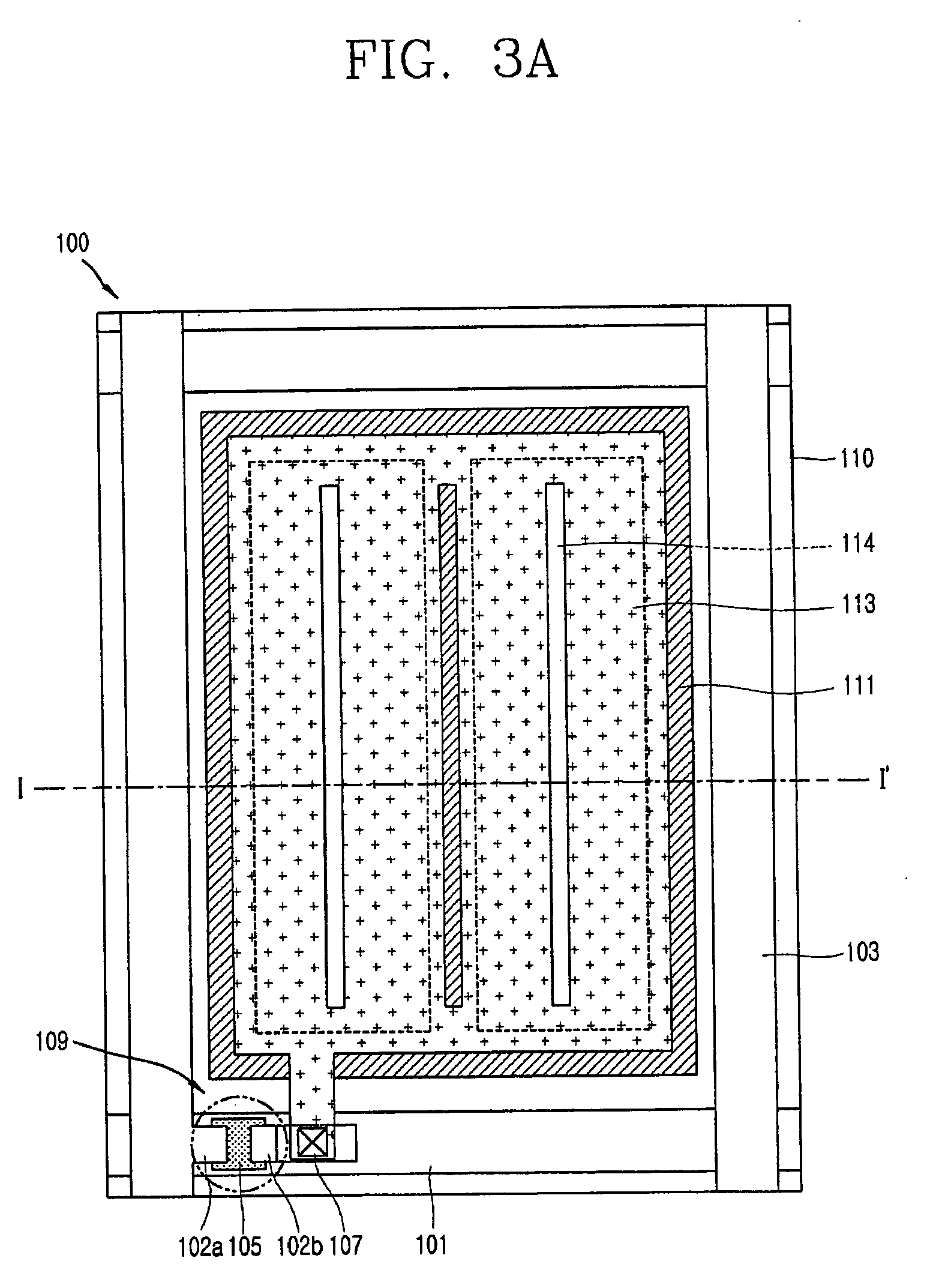
[0038]FIGS. 3A and 3B illustrate an exemplary embodiment of a multi-domain LCD device in accordance with the present invention. FIG. 3A is a plan view showing a unit pixel, and FIG. 3B is a cross-sectional view taken along line I-I′ in FIG. 3A. As shown in FIG. 3B, a multi-domain LCD device 100 (FIG. 3A) includes first and second substrates 110 and 120, and a liquid crystal layer 119 formed therebetween. Also, as shown in FIG. 3A, the first substrate 110 is provided with a plurality of gate lines 101 and a plurality of data lines 103 horizontally and vertically arranged to define pixel regions, and a thin film transistor (TFT)109 formed at each crossing of the gate line 101 and the data line 103. The TFT 109 includes a gate electrode...


PUM


Abstract

A multi-domain LCD device includes first and second substrates, gate and data lines defining a plurality of pixel regions on the first substrate, at least one first electric field distortion unit formed at the pixel region, a pixel electrode formed at the pixel region and having at least one second electric field distortion unit, a common electrode formed on the second substrate, and a liquid crystal layer formed between the first and second substrates, having liquid crystal molecules symmetrically arranged by the first electric field distortion unit and having a plurality of domains generated by the first and second electric field distortion units.

Description

[0001] This application claims the benefit of Korean Application Nos. 2004-87482 and 2005-15550, filed Oct. 29, 2004 and Feb. 24, 2005, respectively, which are hereby incorporated by reference. BACKGROUND OF THE INVENTION [0002] 1. Field of the Invention [0003] The present invention relates to a liquid crystal display (LCD) device and, more particularly, to an LCD device and its fabrication method capable of obtaining a wide viewing angle and enhancing an aperture ratio. [0004] 2. Discussion of the Related Art [0005] The LCD device, which has been well-known as a high picture quality and low power flat panel display device, includes a thin film transistor (TFT) array substrate and a color filter substrate attached with a uniform interval, in which a liquid crystal layer is formed. Further, the TFT array substrate includes pixels arranged in a matrix form, each unit pixel including a TFT, a pixel electrode and a capacitor. The color filter substrate includes a common electrode formed...

Claims


Application Information

Patent Timeline
IPC IPC(8): G02F1/1337
CPCG02F1/133707G02F1/1393G02F2001/134345G02F1/134345
Inventor HONG, HYUNG-KI
Owner LG DISPLAY CO LTD
Why Eureka
Try Eureka