Apparatus to manufacture semiconductor

a technology of apparatus and semiconductor, applied in the direction of coating, chemical vapor deposition coating, metallic material coating process, etc., can solve the problems of difficult to uniformly distribute process gas onto the upper surface of the substrate, and difficult to obtain uniform film formation on the overall surface of the semiconductor substrate, etc., to achieve uniform

Inactive Publication Date: 2006-05-11
SAMSUNG ELECTRONICS CO LTD
View PDF7 Cites 442 Cited by
  • Summary
  • Abstract
  • Description
  • Claims
  • Application Information

AI Technical Summary

Benefits of technology

[0009] Accordingly, the present general inventive concept provides an apparatus to manufacture a semiconductor, which increases a diffusion range of process gases supplied from gas supply nozzles so that the process gases are uniformly distributed onto a reaction region above a semiconductor substrate, thereby uniformly performing a desired processing procedure.

Problems solved by technology

Since the above apparatus is configured such that an outlet of the upper gas supply nozzle has a rectilinear shape, it is difficult to uniformly distribute the process gas onto an upper surface of a substrate due to a concentration of the process gas supplied through the upper gas nozzle onto a central portion of the semiconductor substrate.
Accordingly, it is difficult to obtain a film uniformly formed on the overall surface of the semiconductor substrate, i.e., the film can be concentrated onto the central portion of the semiconductor substrate instead of uniformly formed over all of the surface of the substrate.

Method used


Image

  • Apparatus to manufacture semiconductor
  • Apparatus to manufacture semiconductor
  • Apparatus to manufacture semiconductor

Examples


Embodiment Construction

[0021] Reference will now be made in detail to the embodiment of the present general inventive concept, an example of which is illustrated in the accompanying drawings, wherein like reference numerals refer to like elements throughout. The embodiment is described below to explain the present general inventive concept while referring to the drawings.

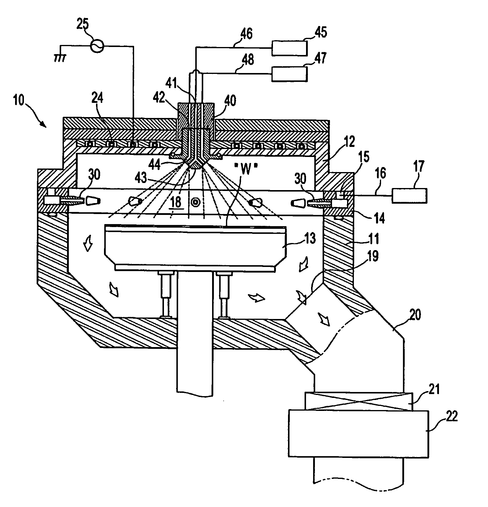
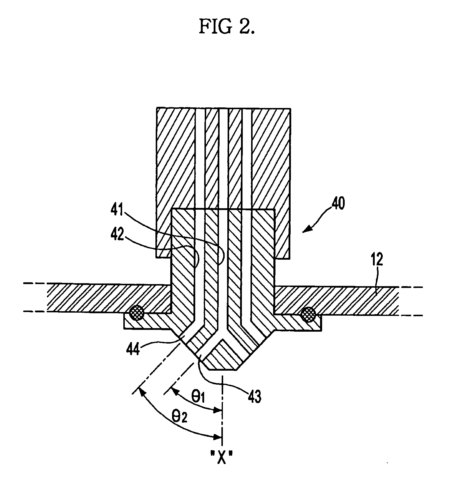
[0022]FIG. 1 is a longitudinal sectional view of an apparatus 10 to manufacture a semiconductor according to an embodiment of the present general inventive concept. Referring to FIG. 1, the apparatus 10 comprises a reaction chamber 18 to perform a fabricating process of a semiconductor substrate W therein, including a cylindrical main body 11 having an opened upper surface and a cover 12 to cover the opened upper surface of the main body 11. Here, the fabricating process performed by the apparatus 10 is either a depositing process to form a thin film on a surface of the semiconductor substrate W, or an etching process to etch the film on...


PUM

PropertyMeasurementUnit
angleaaaaaaaaaa
semiconductoraaaaaaaaaa
concentrationaaaaaaaaaa

Abstract

An apparatus to manufacture a semiconductor, in which distribution of process gases supplied to a reaction region in a reaction chamber is uniform, includes a gas supply nozzle to supply process gases to a semiconductor substrate in the reaction chamber, wherein the gas supply nozzle includes a first supply channel formed in a longitudinal direction, and first outlet channels formed at an outlet of the first supply channel such that the first outlet channels are inclined with respect to the direction of the first supply channel at a designated angle to diffuse the process gas supplied through the first supply channel.

Description

CROSS-REFERENCE TO RELATED APPLICATIONS [0001] This application claims the benefit under 35 U.S.C. § 119 of Korean Patent Application No. 2004-91828, filed November 11, 2004, in the Korean Intellectual Property Office, the disclosure of which is incorporated herein in its entirety by reference. BACKGROUND OF THE INVENTION [0002] 1. Field of the Invention [0003] The present general inventive concept relates to an apparatus to manufacture a semiconductor, and more particularly, to an apparatus to manufacture a semiconductor having an improved gas supply nozzle so that process gases are uniformly sprayed onto a semiconductor substrate. [0004] 2. Description of the Related Art [0005] Generally, when a conventional depositing or etching process is performed during manufacturing of a semiconductor, reactive process gas is supplied to the inside of a reaction chamber in a vacuum state, and then high-frequency power is supplied to the inside of the reaction chamber so that the process gas i...

Claims


Application Information

Patent Timeline
Patent Type & Authority Applications(United States)
IPC IPC(8): C23C16/00
CPCC23C16/45574C23C16/45578H01L21/02
Inventor CHOI, JIN HYUK
Owner SAMSUNG ELECTRONICS CO LTD
Why Eureka
Try Eureka