Dry etching apparatus

Inactive Publication Date: 2006-05-11
DONGBU ELECTRONICS CO LTD
View PDF3 Cites 32 Cited by
  • Summary
  • Abstract
  • Description
  • Claims
  • Application Information

AI Technical Summary

Benefits of technology

[0023] An object of the present invention is to provide a plasma etching and/or cleaning apparatus including a material resistant to plasma etching so as to reduce particles in the etching and/

Problems solved by technology

In the step of fabricating a wafer, which is formed by processes of developing and etching a circuit pattern on a wafer surface, particles such as fine dust or moisture must be thoroughly removed because they may disturb and damage the formation of the circuit pattern.
However, particles that may be produced due to internal factors during the fabrication process cannot be easily prevented beforehand.
However, management of the wet washing process is difficult, the cost required for the washing liquid increases the production cost, and the running time is long, thereby reducing productivity.
The quartz insulator 16 can be easily damaged even by the smallest impact, and its basic material is frequently damaged during the washing processes.
Then, the electrons or ions

Method used


Image

  • Dry etching apparatus
  • Dry etching apparatus

Examples


Embodiment Construction

[0030] Reference will now be made in detail to the preferred embodiments of the present invention, examples of which are illustrated in the accompanying drawings. Wherever possible, the same reference numbers will be used throughout the drawings to refer to the same or like parts.

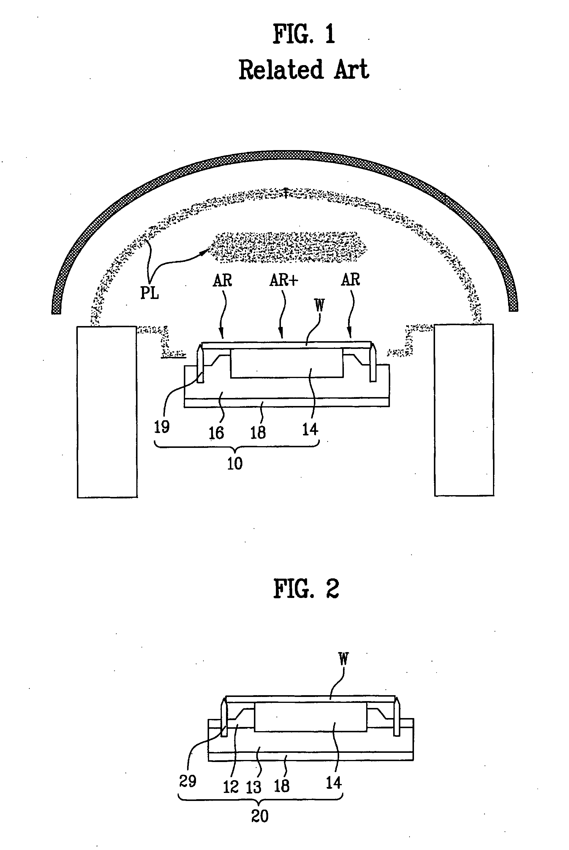
[0031]FIG. 2 illustrates a general cross-sectional view showing main parts of a plasma etching apparatus according to the present invention. The elements that are identical to the elements shown in FIG. 1 will be given the same reference numerals, and the description of the same will be omitted for simplicity.

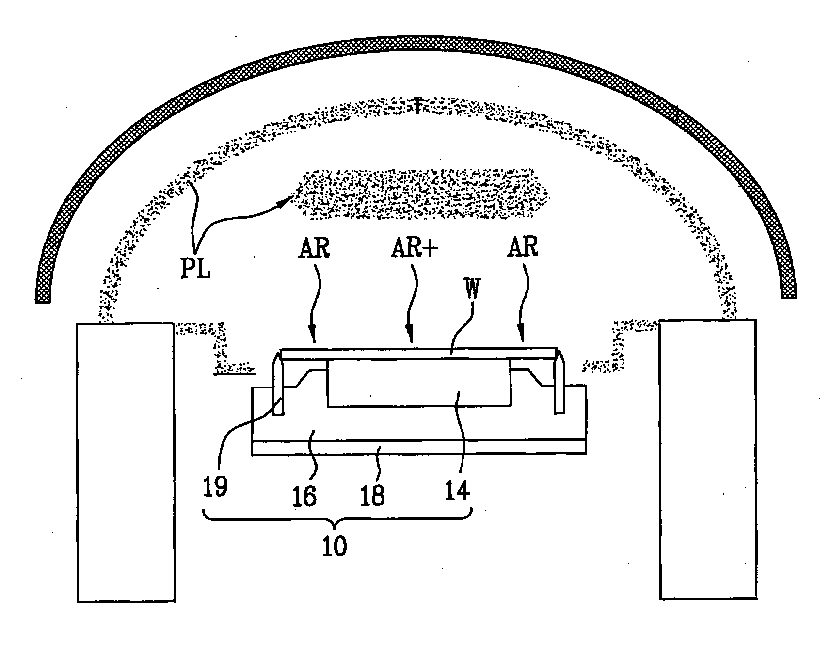
[0032] As shown in FIG. 2, the dry etching apparatus according to the present invention includes a loading unit 20. The loading unit 20 comprises an upper pedestal 14 supporting a wafer (W) on its upper surface, a quartz insulator 13 and a ceramic cover 12 thereon, and a lower pedestal 18 contacting and supporting a lower surface of the quartz insulator.

[0033] The upper pedestal 14 may comprise or c...


PUM

PropertyMeasurementUnit
Lengthaaaaaaaaaa
Diameteraaaaaaaaaa
Depthaaaaaaaaaa

Abstract

A plasma etching and/or cleaning apparatus is disclosed. The apparatus includes a pedestal for mounting a wafer thereon, a quartz insulator having the pedestal therein, a ceramic top cover covering a portion of the quartz insulator that is exposed to plasma, and a lower pedestal supporting the quartz insulator. By simply covering the quartz insulator with a ceramic cover, a decrease in particles may be observed, and the lifetime of the quartz pedestal is increased. Therefore, maintenance and repair costs of the apparatus can be reduced, thereby enhancing operation efficiency. Furthermore, since the production of particles can be reduced, a more uniform etch rate can be obtained when etching the wafer, thereby enhancing the yield of the semiconductor device. In a further embodiment, the ceramic cover has an upper surface free of holes adapted to contain an alignment pin.

Description

[0001] This application claims the benefit of Korean Patent Application No. P2004-90726, filed on Nov. 09, 2004, which is hereby incorporated by reference as if fully set forth herein. BACKGROUND OF THE INVENTION [0002] 1. Field of the Invention [0003] The present invention relates to a dry etching and / or cleaning apparatus, and more particularly, to a plasma etching and / or cleaning apparatus that can etch and / or clean a semiconductor wafer using plasma, wherein particles accumulated on edge portions of a wafer and / or elsewhere in the apparatus may be reduced. [0004] 2. Discussion of the Related Art [0005] In order to fabricate a semiconductor device, a wafer is formed and treated that may contain a polycrystalline silicon formed from, e.g., high purity amorphous silicon. Subsequently, a process of selecting the treated wafer is performed. In order to treat the wafer, unit processes (e.g., a photo process, an etching process, an expansion process, and a thin film process) are perfor...

Claims


Application Information

Patent Timeline
IPC IPC(8): H01L21/306
CPCH01J37/32477H01J37/32559H01J37/32623H01L21/67069H01L21/68757H01L21/3065
Inventor KIM, JONG HUN
Owner DONGBU ELECTRONICS CO LTD
Why Eureka
Try Eureka