Test structure design for reliability test

Inactive Publication Date: 2006-05-25
APPLIED MATERIALS INC
View PDF3 Cites 10 Cited by
  • Summary
  • Abstract
  • Description
  • Claims
  • Application Information

AI Technical Summary

Benefits of technology

[0010] The present invention generally provides semiconductor test structures that facilitate the evaluation of multiple design parameters and a method utilizing such a test structure.
[0011] One embodiment provides a test structure for determining the reliability of conductive lines formed in a semiconductor substrate. The test structure generally includes at least one conductive line formed in a first metal layer of the semiconductor substrate and one or more thermal stress-inducing test pads formed in a second metal layer of the semiconductor substrate, wherein each of the test pads is wider in at least two dimensions than a line width of the conductive line. One or more vias electrically and mechanically couple the first one or more test pads to the first conductive line. A plurality of probe contact pads are electrically coupled to the first conductive line at different locations, and allow the measurement of at least one of line resistance of the first conductive line or the resistance across one or more of the vias.
[0012] Another embodiment provides another test structure for determining the reliability of conductive lines formed in a semiconductor substrate. The test structure generally includes at least one conductive line formed in a first metal layer of the semiconductor substrate and one or more thermal stress-inducing test pads formed in a second metal layer of the semiconductor substrate, wherein each of the test pads is wider in a

Problems solved by technology

As these conductive lines shrink in width, the conductive lines become more susceptible to effects, such as electromigration, which may result in voids formatting in the conductive lines.
A void generally refers to a decrease in the volume of metal in the conductive path of the line that results in increased line resistance which may in turn lead to signal degradation and, ultimately, device failure.
In other words, due to the complex nature of the physical stresses on a conductive line, characterizing or predicting the stresses caused by any particular combination of design parameters is extremely difficult.
The simple design of the conventional test structures limits their utility to test different combinations of parameters.
However, constructing multiple test structures is time consuming and expensive.

Method used


Image

  • Test structure design for reliability test
  • Test structure design for reliability test
  • Test structure design for reliability test

Examples


Embodiment Construction

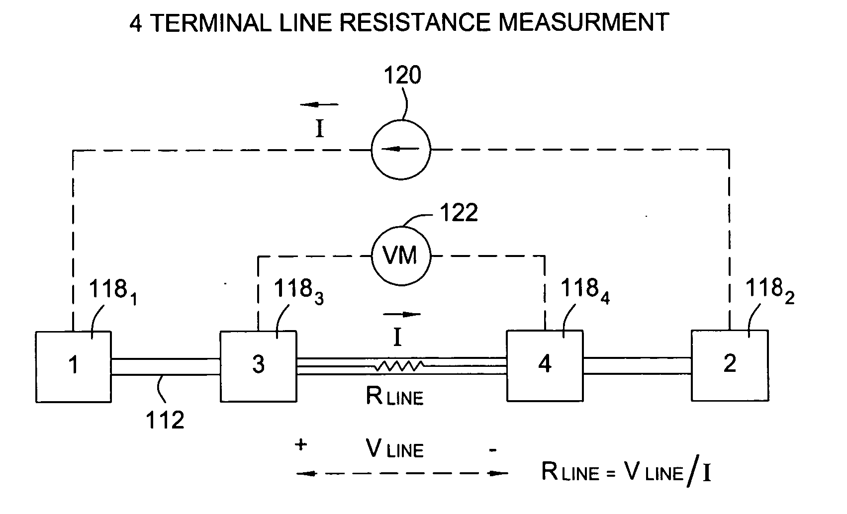
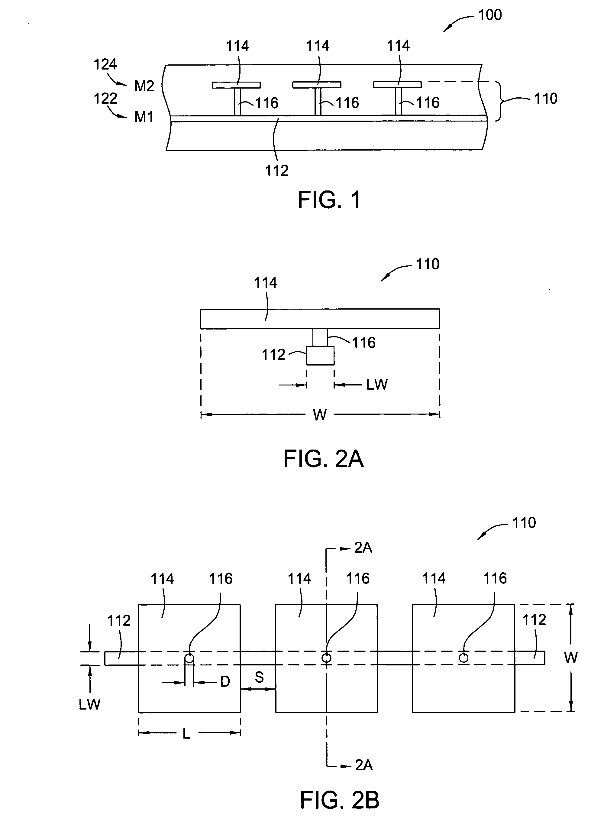
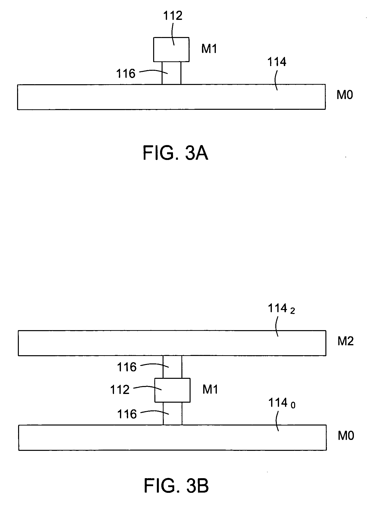
[0020] The present invention generally provides a flexible semiconductor test structure that may be incorporated into a semiconductor device. The test structure may include a plurality of test pads designed to physically stress conductive lines to which they are attached during thermal cycling. In some applications, by utilizing test pads with different dimensions (lengths and / or widths), the effects of thermal stress generated by a plurality of conductive lines having corresponding different dimensions may be simulated. As a result, designers may utilize such test structures to determine design parameters (e.g., line / via widths, densities, and ratios) that should result in a device which operates reliably over its expected lifetime. By evaluating multiple combinations of such parameters with a single test structure, development costs and the time it typically takes to bring such a device to market may both be reduced significantly.

AN EXEMPLARY TEST STRUCTURE

[0021]FIG. 1 illustrat...


PUM


Abstract

A flexible semiconductor test structure that may be incorporated into a semiconductor device is provided. The test structure may include a plurality of test pads designed to physically stress conductive lines to which they are attached during thermal cycling. By utilizing test pads with different dimensions (lengths and / or widths), the effects of thermal stress generated by a plurality of conductive lines having corresponding different dimensions may be simulated.

Description

BACKGROUND OF THE INVENTION [0001] 1. Field of the Invention [0002] Embodiments of the present invention generally relate to semiconductor manufacturing and, more particularly, to test structures formed in a semiconductor device useful in evaluating possible device design parameters. [0003] 2. Description of the Related Art [0004] In a semiconductor device, an interconnect structure consisting of a network of conductive lines connected by vias transmitting signals among various layers of the device. As circuit dimensions shrink to provide devices with more and more functionality, the conductive lines used in interconnect structures decrease in width accordingly. As these conductive lines shrink in width, the conductive lines become more susceptible to effects, such as electromigration, which may result in voids formatting in the conductive lines. Physical stresses can also form the voids, such as thermal stresses resulting from differences in temperature coefficients between dielect...

Claims


Application Information

Patent Timeline
IPC IPC(8): G01R31/26
CPCG01R31/2831G01R31/2853G01R31/2856H01L22/34H01L2924/0002H01L2924/00
Inventor YOSHIDA, NAOMINAGATA, TOSHIYUKI
Owner APPLIED MATERIALS INC
Why Eureka
Try Eureka