
System and method for compensating for the effects of process, voltage, and temperature variations in a circuit

a circuit and voltage compensation technology, applied in logic circuits, oscillation generators, reliability increasing modifications, etc., can solve problems such as less than optimal, electrical characteristics that vary, and consume unacceptable amounts of ic's real esta

Inactive Publication Date: 2006-06-01
AVAGO TECH INT SALES PTE LTD
View PDF17 Cites 3 Cited by
  • Summary
  • Abstract
  • Description
  • Claims
  • Application Information

AI Technical Summary

Benefits of technology

The present invention provides an apparatus for controlling the output current of I / O circuits independent of PVT conditions. This is achieved by making the gate drive and the effective width of the output driver p-channel metal oxide semiconductor and n-channel metal oxide semiconductor dependent on the rate of rise of a sense voltage. This keeps the pad voltage rise and fall time relatively independent of fabrication process, supply-voltage, and temperature. The technical effect of this invention is to improve the stability and reliability of the output current drive of I / O circuits.

Problems solved by technology

A critical challenge in the design, fabrication, and operation of these I / O circuits is that their electrical characteristics may vary depending on the particular PVT conditions.
Traditional approaches for ensuring that the electrical characteristics of I / O circuits remain independent of PVT conditions include complicated switching arrangements.
These traditional approaches, however, consume unacceptable amounts of the IC's real estate and are therefore less than optimal.

Method used


Image

  • System and method for compensating for the effects of process, voltage, and temperature variations in a circuit
  • System and method for compensating for the effects of process, voltage, and temperature variations in a circuit
  • System and method for compensating for the effects of process, voltage, and temperature variations in a circuit

Examples


Embodiment Construction

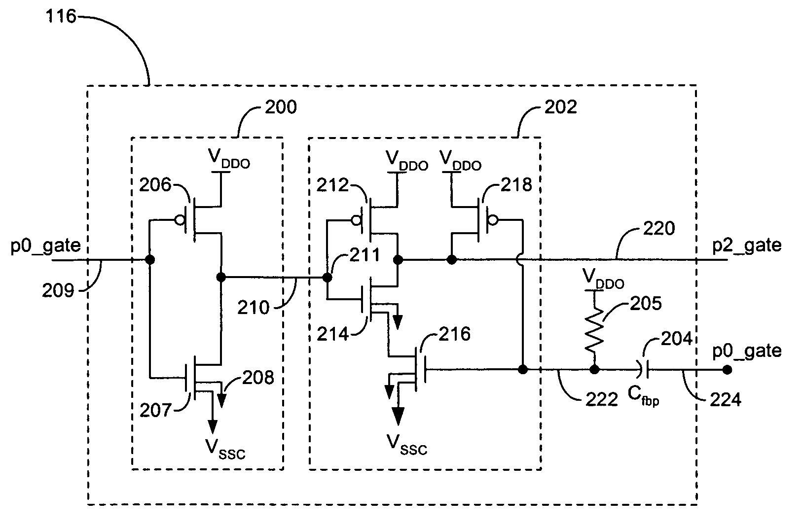
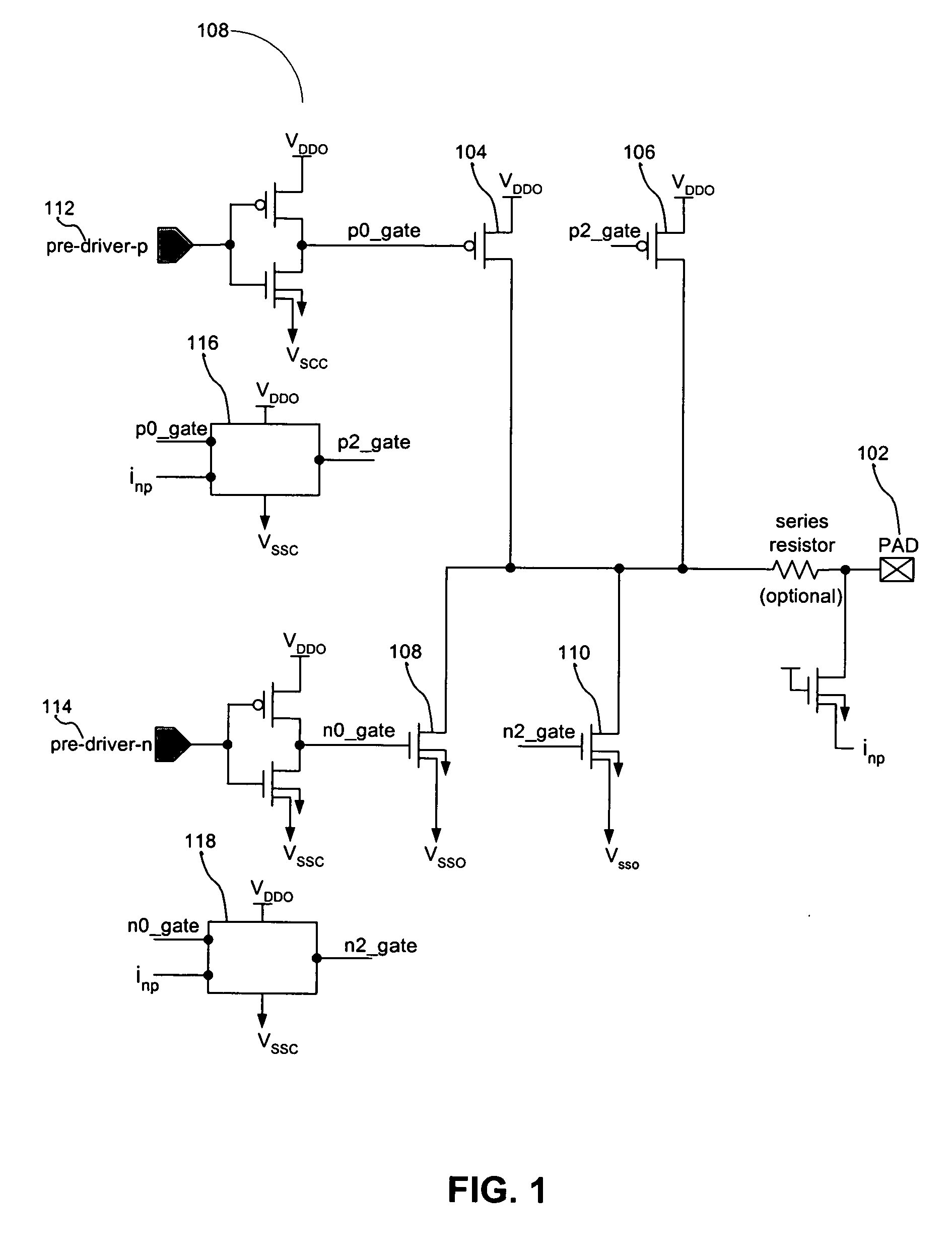
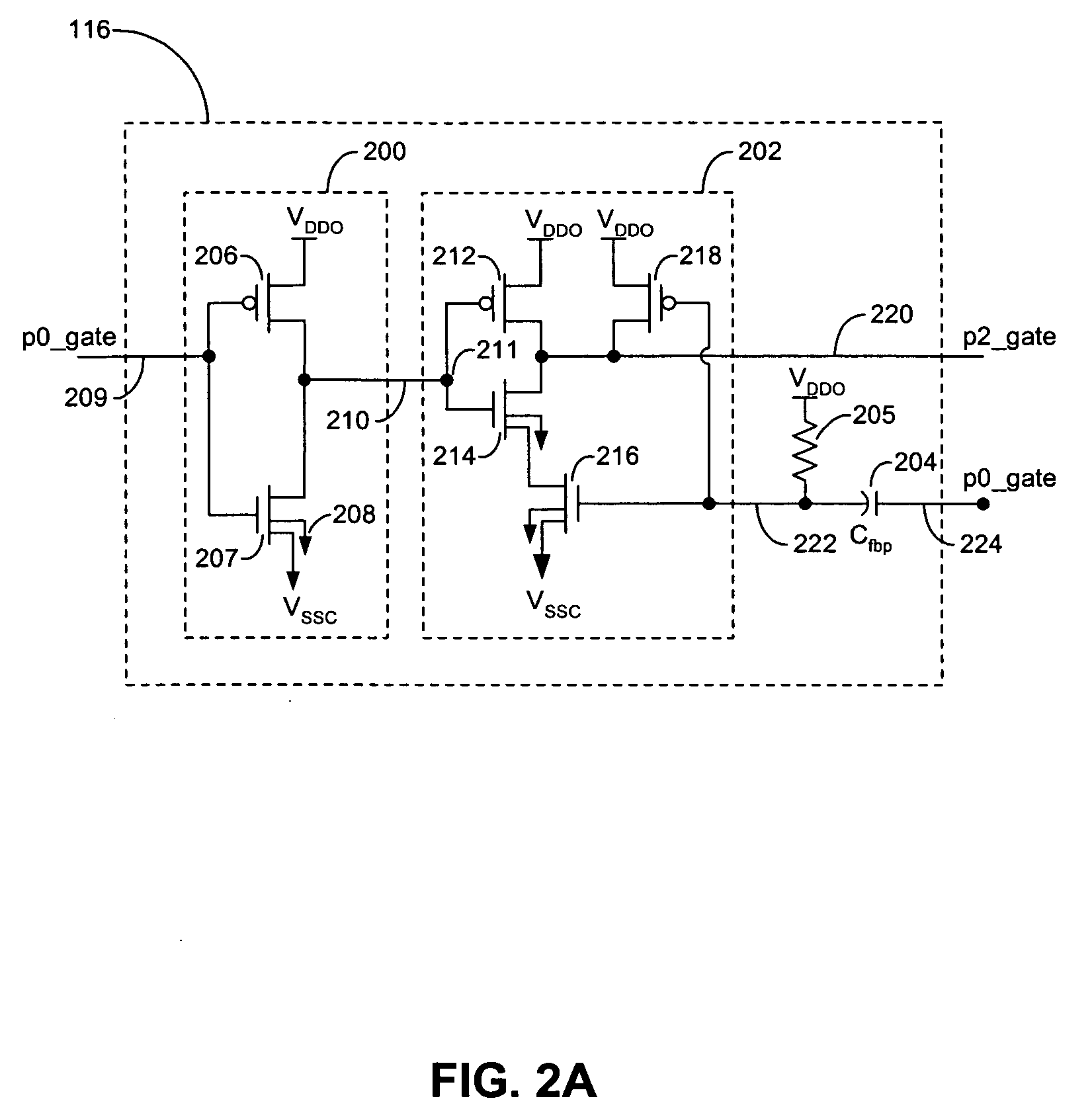
[0021] The following detailed description of the present invention refers to the accompanying drawings that illustrate exemplary embodiments consistent with this invention. Other embodiments are possible, and modifications may be made to the embodiments within the spirit and scope of the present invention. Therefore, the following detailed description is not meant to limit the invention. Rather, the scope of the invention is defined by the appended claims.

[0022] It would be apparent to one of skill in the art that the present invention, as described below, may be implemented in many different embodiments of hardware, software, firmware, and / or the entities illustrated in the figures. Any actual software code with specialized control hardware to implement the present invention is not limiting of the present invention. Thus, the operation and behavior of the present invention will be described with the understanding that modifications and variations of the embodiments are possible, g...


PUM


Abstract

A system and method for compensating for process, voltage, and temperature variations in a circuit is provided. A system includes an inverter having an input port, and an output port, and is configured to (i) receive an input signal, (ii) delay the received input signal, and (iii) provide the delayed signal to the inverter output port. The system also includes a logic device including at least two input ports and an output port. A first of the at least two input ports is configured to receive the delayed signal. Finally, the system includes a charge storing device having a first end coupled, at least indirectly, to a second of the at least two input ports and a second end coupled to a logic device common node. The charge storing device is configured to (i) receive the input signal and (ii) sense a rate of change in voltage of the received input signal, the sensed voltage being representative of a corresponding current. The logic device output port is configured to output an output signal responsive to the delayed signal and the corresponding current.

Description

CROSS-REFERENCE TO RELATED APPLICATIONS [0001] The present application is a Divisional of U.S. Non-Provisional application Ser. No. 10 / 293,259, filed Nov. 14, 2002, which claims the benefit of U.S. Provisional Application No. 60 / 361,033, filed Mar. 1, 2002, all of which is incorporated by reference herein in its entirety.BACKGROUND OF THE INVENTION [0002] 1. Field of the Invention [0003] The present invention relates generally to controlling electrical characteristics associated with input / output (I / O) circuits. More particularly, the present invention relates to developing I / O circuits having electrical characteristics, such as operating frequencies, that are independent of variations in fabrication process, supply-voltage, and temperature (PVT) conditions. [0004] 2. Related Art [0005] I / O circuits are used to interface traditional integrated circuits (ICs) with electrical environments external to the IC. The I / O circuit acts as a driver for signals generated by the IC and provides...

Claims


Application Information

Patent Timeline
Patent Type & Authority Applications(United States)
IPC IPC(8): H03B1/00H03K19/003
CPCH03K19/00384
Inventor AJIT, JANARDHANAN S.
Owner AVAGO TECH INT SALES PTE LTD
Learn More