System and method for recalibrating flat panel field emission displays

a flat panel field and display technology, applied in the field of display screens, can solve the problems of not necessarily uniform beams of electronic structures for each pixel in the fed

Inactive Publication Date: 2006-06-01
SONY CORP +1
View PDF15 Cites 11 Cited by
  • Summary
  • Abstract
  • Description
  • Claims
  • Application Information

AI Technical Summary

Benefits of technology

[0005] The present invention provides a system and method for measuring and correcting the non-uniform pixels of ...

Problems solved by technology

However, unlike conventional CRT displays that use a single or in some cases three electron beams to scan across the phosphor screen in a raster pattern, FEDs use...

Method used


Image

  • System and method for recalibrating flat panel field emission displays
  • System and method for recalibrating flat panel field emission displays
  • System and method for recalibrating flat panel field emission displays

Examples


Embodiment Construction

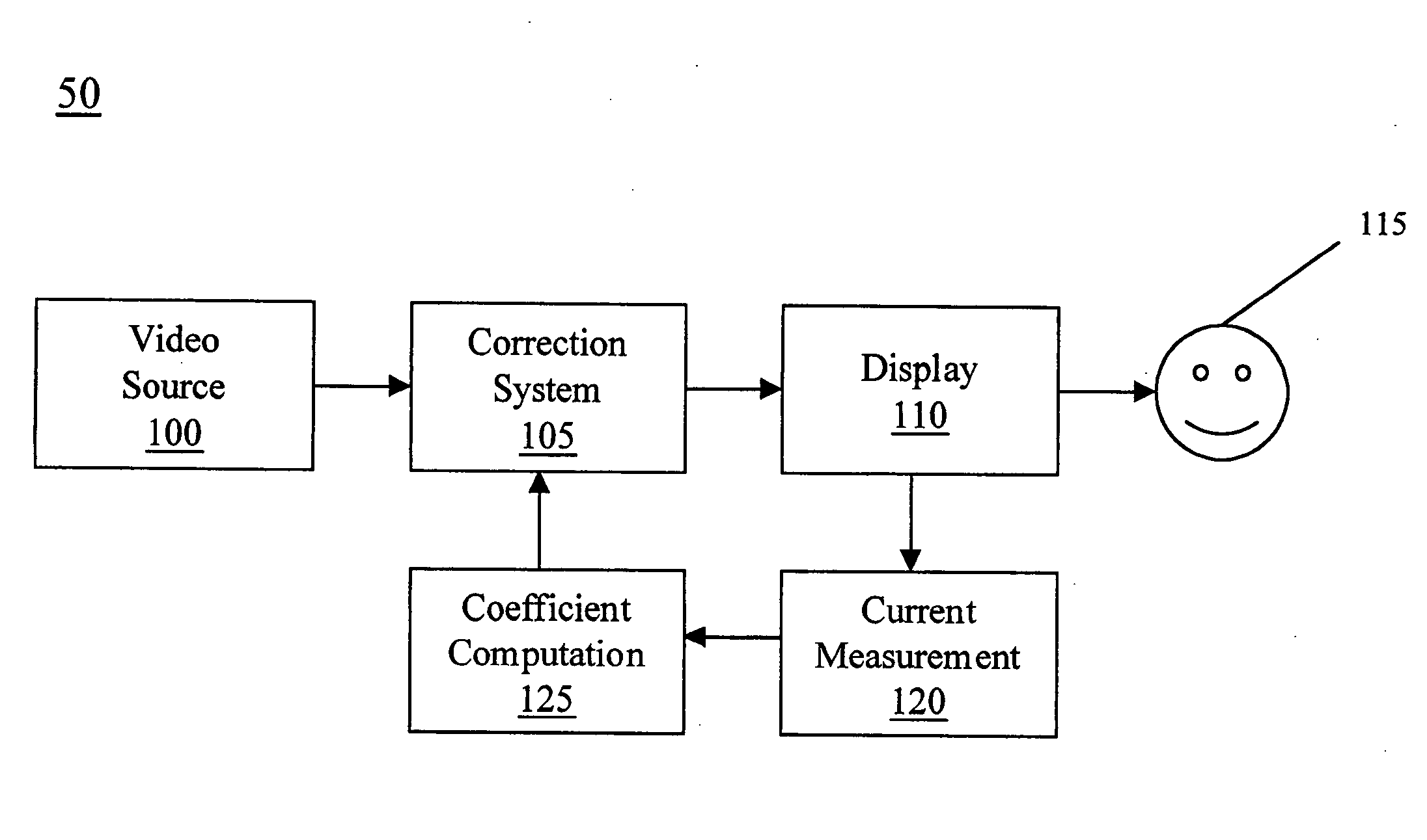
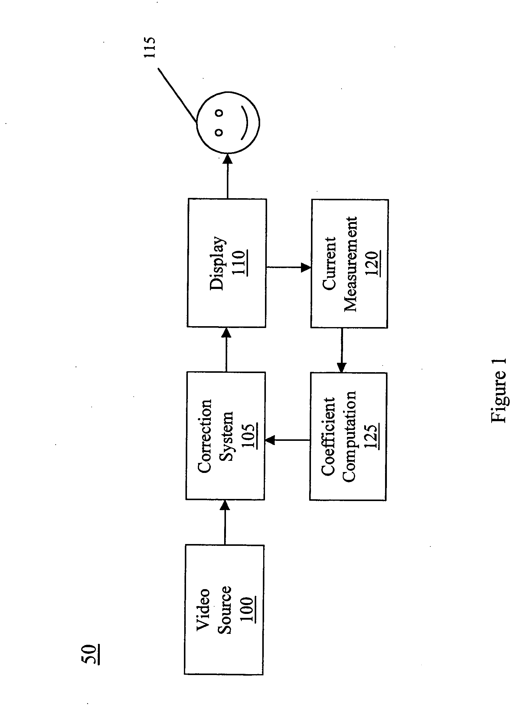
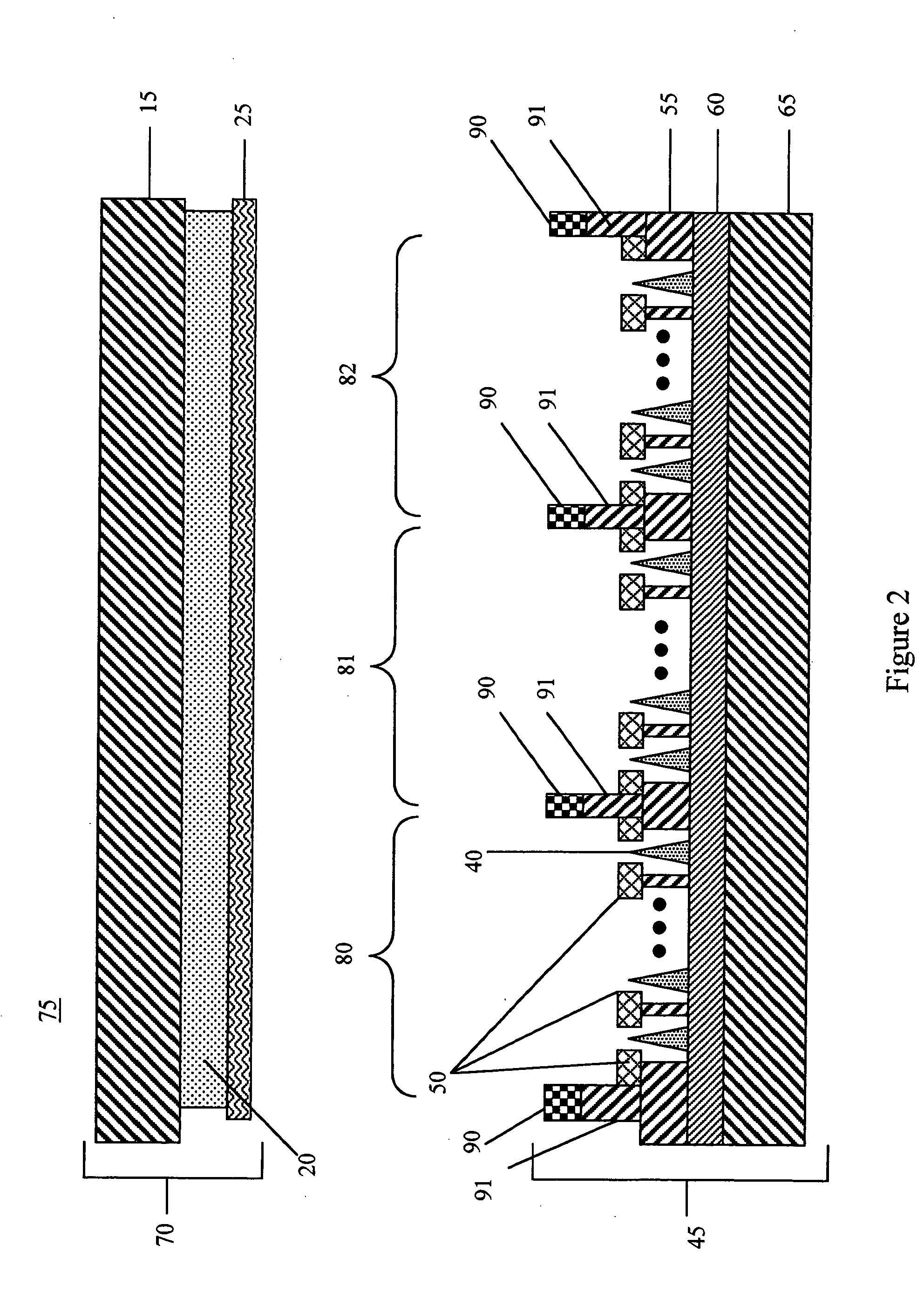
[0034] Reference will now be made in detail to the present embodiments of the invention, examples of which are illustrated in the accompanying drawings. While the invention will be described in conjunction with the present embodiments, it will be understood that they are not intended to limit the invention to these embodiments. On the contrary, the invention is intended to cover alternatives, modifications and equivalents, which may be included within the spirit and scope of the invention as defined by the appended claims. Furthermore, in the following description, for purposes of explanation, numerous specific details are set forth in order to provide a thorough understanding of the present invention. It will be apparent, however, to one skilled in the art, upon reading this disclosure, that the present invention may be practiced without these specific details. In other instances, well-known structures and devices are not described in detail in order to avoid obscuring aspects of t...


PUM


Abstract

A field emission display (FED) having a correction system with a correction coefficient derived from emission current is presented. Within one embodiment in accordance with the present invention, a field emission display has an anode at the faceplate and a focus structure. The anode potential is held at ground while the focus structure potential is held between, but is not limited to, 40 and 50 volts. The current flowing to the focus structure is measured and used as the basis for the correction coefficient for the field emission display.

Description

TECHNICAL FIELD [0001] The present invention relates to the field of display screens. More specifically, the present invention relates to the field of, but is not limited to, flat panel field emission displays (FEDs) and / or cathode ray tube (CRT) displays. BACKGROUND ART [0002] Flat panel field emission displays (FEDs), like standard cathode ray tube (CRT) displays, generate light by impinging high-energy electrons on a picture element. (pixel) of a phosphor screen. The excited phosphor then converts the electron energy into visible light. However, unlike conventional CRT displays that use a single or in some cases three electron beams to scan across the phosphor screen in a raster pattern, FEDs use stationary electron beams for each color element of each pixel. This allows the distance from the electron source to the screen to be very small compared to the distance required for the scanning electron beams of the conventional CRTs. In addition, the vacuum tube of the FED can be made...

Claims


Application Information

Patent Timeline
IPC IPC(8): G09G3/22H04N5/68G09G3/20G09G5/00G09G5/02G09G5/36
CPCG09G3/2011G09G3/2014G09G3/22Y10S345/904G09G2310/06G09G2320/0285G09G2320/029G09G5/02G09G3/20
Inventor HANSEN, RONALD L.DUNPHY, JAMES C.SPINDT, CHRISTOPHER J.CLEEVES, JAMES M.TRUPPA, JEROME M.FINK, GREGORY M.IGUCHI, YUKINOBU
Owner SONY CORP
Why Eureka
Try Eureka