Pixel circuit and light emitting display

a technology of light emitting display and pixel circuit, which is applied in the field can solve the problems of deteriorating aperture ratio of light emitting display and complicated wiring lines, and achieve the effect of improving the aperture ratio of light emitting display and reducing the number of pixel circuits

Active Publication Date: 2006-06-01
SAMSUNG DISPLAY CO LTD
View PDF9 Cites 65 Cited by
  • Summary
  • Abstract
  • Description
  • Claims
  • Application Information

AI Technical Summary

Benefits of technology

[0015] Accordingly, one aspect of the present invention provides light emitting displays, in which two adjacent pixel circuits coupled to one scan line share one pixel power supply line and a plurality of OLEDs are coupled to one pixel circuit so that it is possible to reduce the number of pixel circuits and the number of wiring lines of the light emitting display and thus improve the aperture ratio of the light emitting display.

Problems solved by technology

Also, because one emission control line and a pixel power supply line are coupled to each pixel row, wiring lines become complicated and the aperture ratio of the light emitting display deteriorates.

Method used


Image

  • Pixel circuit and light emitting display
  • Pixel circuit and light emitting display
  • Pixel circuit and light emitting display

Examples


first embodiment

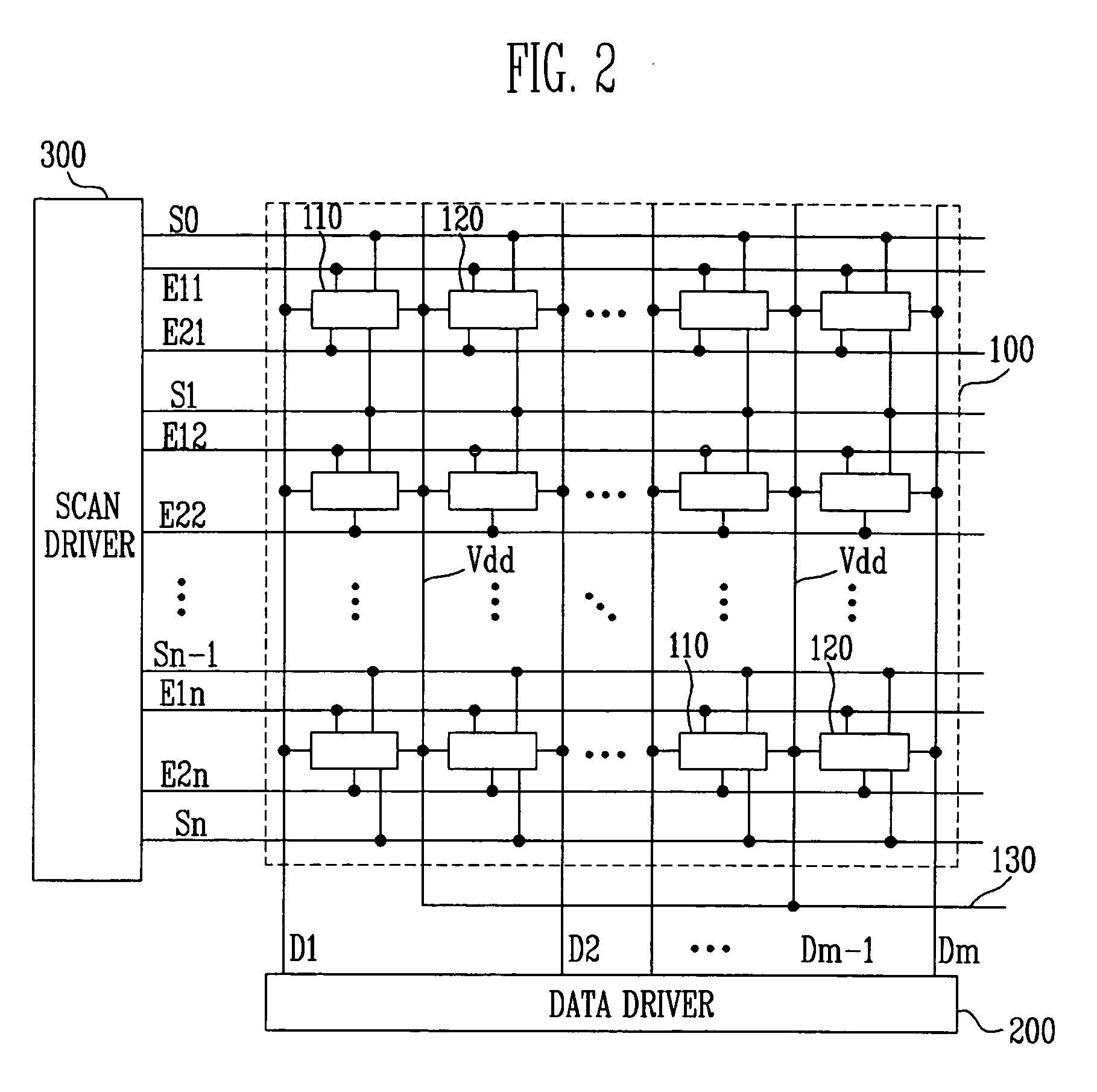
[0026]FIG. 2 illustrates a light emitting display according to the present invention. The light emitting display includes an image display unit 100, a data driver 200, and a scan driver 300.

[0027] The image display unit 100 includes a plurality of pixels 110, 120 including a plurality of OLEDs, a plurality of scan lines S0, S1, S2, . . . , Sn−1, Sn arranged in a row direction, a plurality of first emission control lines E11, E12, . . . , E1n−1, Em and second emission control lines E21, E22, . . . , E2n−1, E2n arranged in the row direction, a plurality of data lines D1, D2, . . . , Dm−1, Dm arranged in a column direction, and a plurality of pixel power supply lines Vdd for supplying pixel power.

[0028] Each one pixel power supply line Vdd is simultaneously coupled to two adjacent pixels 110 (or to two adjacent pixels 120) in the row direction so that the number of required pixel power supply lines Vdd is reduced to half of the number of pixels. Therefore, it is possible to reduce the...

second embodiment

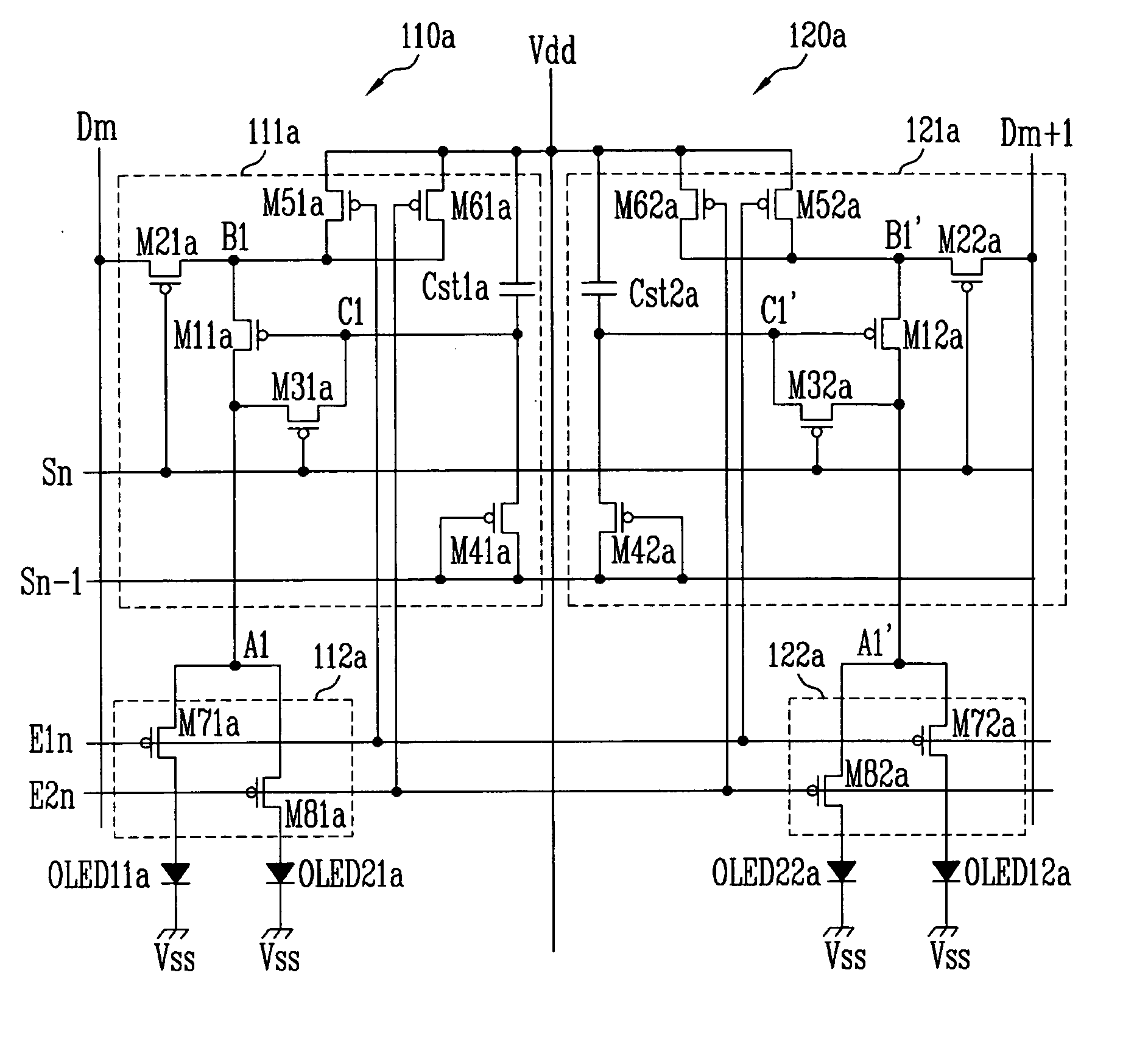
[0045]FIG. 4 is a circuit diagram illustrating the pixel circuit used for the light emitting display of the present invention. The pixels including two adjacent pixel circuits coupled to one scan line are illustrated. In the second pixel circuit, the left pixel is referred to as the first pixel 110b and the right pixel is referred to as the second pixel 120b.

[0046] Each of the first and second pixels 110b, 120b include a driving circuit and a switching circuit. The driving circuit 111b, 121b includes elements that are coupled to the scan lines Sn, Sn−1 and are driven by the scan signals sn, sn−1. The switching circuit 112b, 122b includes switching elements that are coupled to the emission control lines E1n, E2n and are driven by the emission control signals e1n, e2n. The switching circuit 112b, 122b couples the driving circuit 111b, 121b to the OLEDs and controls the flow of current to these OLEDs.

[0047] In the first pixel 110b, the drain of the first transistor M1b is coupled to ...

third embodiment

[0070]FIG. 7 is a circuit diagram illustrating the pixel circuit used for the light emitting display of the present invention. The third pixel circuit includes two adjacent pixel circuits 110c, 120c coupled to one scan line. The left pixel is referred to as the first pixel 110c and the right pixel is referred to as the second pixel 120c.

[0071] Each of the first and second pixels 110c, 120c include a driving circuit and a switching circuit. The driving circuit 111c, 121c includes elements that are coupled to the scan lines Sn, Sn−1 and are driven by the scan signals sn, sn−1. The switching circuit 112c, 122c includes switching elements that are coupled to the emission control lines E1n, E2n and are driven by the emission control signals e1n, e2n. The switching circuit 112c, 122c couples the driving circuit 111c, 121c to the OLEDs and controls the flow of current to these OLEDs.

[0072] The first and second pixels 110c, 120c share the fourth transistor M41c that transmits the initiali...


PUM


Abstract

A pixel circuit for a light emitting display. Adjacent pixels of the light emitting display coupled to one scan line share one first power supply line. A driving circuit in each pixel circuit drives first and second organic light emitting diodes (OLEDs). A switching circuit is coupled between the first and second OLEDs and the driving circuit to sequentially control the driving of the first and second OLEDs. Because two adjacent pixel circuits share one pixel power supply line and a plurality of OLEDs are coupled to one pixel circuit, it is possible to reduce the number of pixel circuits and the number of wiring lines of the light emitting display. Other circuit elements may also be shared between adjacent pixel circuits. Reducing the wiring and other elements of the pixel circuits makes it possible to increase the aperture ratio of the light emitting display.

Description

CROSS-REFERENCE TO RELATED APPLICATION [0001] This application claims priority to and the benefit of Korean Patent Application No. 10-2004-95984, filed on Nov. 22, 2004, in the Korean Intellectual Property Office, the entire content of which is incorporated herein by reference. BACKGROUND [0002] 1. Field of the Invention [0003] The present invention relates to a light emitting display, and more particularly to a pixel circuit coupled to a plurality of organic light emitting diodes (OLED) that emit light so that it is possible to improve the aperture ratio of the light emitting display, to compensate for the threshold voltage, and to thus make brightness uniform and a light emitting display using the same. [0004] 2. Discussion of Related Art [0005] Recently, various flat panel displays of lower weight and volume compared with cathode ray tubes (CRT) have been developed. In particular, light emitting displays having improved luminous efficiency, brightness, view angle, and high respon...

Claims


Application Information

Patent Timeline
Patent Type & Authority Applications(United States)
IPC IPC(8): G09G3/30
CPCG09G3/3233G09G2300/0439G09G2300/0465G09G2300/0804G09G2300/0819G09G2300/0842G09G2300/0861G09G2320/043G09G3/30
Inventor KWAK, WON KYUPARK, SUNG CHEON
Owner SAMSUNG DISPLAY CO LTD
Why Eureka
Try Eureka