Pixel circuit, and display device and driving method therefor

a technology of display device and pixel circuit, which is applied in the direction of semiconductor devices, instruments, electrical apparatus, etc., can solve the problems of achieving higher resolution and difficulty in being increased in size, and achieve the effect of reducing the contents of the circuit in the data-side driving circuit, reducing the number of data lines, and reducing the number of pixel circuits

Inactive Publication Date: 2019-01-10
SHARP KK
View PDF14 Cites 22 Cited by
  • Summary
  • Abstract
  • Description
  • Claims
  • Application Information

AI Technical Summary

Benefits of technology

[0075]In a display device including pixel circuits according to the first aspect of the disclosure, the prescribed number of display elements configured to emit lights of the prescribed number of primary colors are included in each of the pixel circuits, the prescribed number being three or more. The display element in a lit state is sequentially switched among the prescribed number of display elements in each pixel circuit in each frame period, and thereby a color image is displayed by sequential additive color mixture. With this configuration, the number of pixel circuits and the area of a display necessary to display a color image at certain resolution (number of pixels) can be significantly reduced in comparison with a known method of forming each pixel of a color image to be displayed by using a certain number of pixel circuits at the same resolution, the certain number being equal to the number of primary colors. Moreover, such a reduction in number of pixel circuits also reduces the number of data lines accordingly, and hence the contents of circuits in a data-side driving circuit is also significantly reduced. Moreover, in a case where the monitor control transistor is included in each pixel circuit to provide a configuration of measuring a current or a voltage in each pixel circuit as in the disclosure, i.e., a case of employing an external compensation method, a circuit (measurement unit circuit) for measurement is provided for each data line in the data-side driving circuit, and hence effects of the reduction in contents of circuits in the data-side driving circuit as a result of the reduction in number of pixel circuits as above are more significant. Hence, it is possible to significantly reduce not only the number of pixel circuits necessary to display a color image at the same resolution as that in a known case but also the contents of circuits in the data-side drive circuit, which makes it possible to display a high-resolution color image while suppressing an increase in cost in an active matrix display device using the external compensation method.
[0076]The display device according to the second aspect of the disclosure is an active matrix display device using the external compensation method including pixel circuits according to the first aspect of the disclosure and configured to display a color image in a field sequential method, and exerts similar effects to those according to the first aspect of the disclosure.
[0077]According to a third aspect of the disclosure, in a case where a color image is displayed on the basis of input signals from an external unit without measuring a current or a voltage in each pixel circuit (in a case of acting in a normal display mode), each frame period is divided into a prescribed number of subframe periods corresponding to the prescribed number of primary colors, the plurality of writing control lines are sequentially turned into an active state in each subframe period while signals representing an image of the primary color corresponding to the subframe period are applied to the plurality of data lines as a plurality of data signals, and each pixel data indicating the image of the primary color is written into the corresponding pixel circuit and held as a data voltage. Moreover, the prescribed number of light emission control transistors in each pixel circuit are sequentially turned into an ON state at respective prescribed intervals in each frame period. Consequently, the prescribed number of display elements in each pixel circuit are sequentially turned into a lit state for respective prescribed periods (one subframe periods, normally) to emit light at the intensity corresponding to the written pixel data. In this way, the color image represented by the input signals is displayed by sequential additive color mixture. The display device according to the third aspect of the disclosure for displaying a color image in a field sequential method is also an active matrix display device using the external compensation method including pixel circuits according to the first aspect of the disclosure, and exerts similar effects to those according to the first or second aspect of the disclosure.
[0078]In the fourth aspect of the disclosure, the light emission control line driving circuit is configured by one demultiplexer provided so as to correspond to each writing control line, the light emission control line activation circuit configured to output a light emission enable signal to each demultiplexer, one pull-down transistor provided for each light emission control line, and the light emission control line deactivation circuit configured to control on / off of each pull-down transistor. Each light emission enable signal output from the light emission control line activation circuit is supplied to the prescribed number of light emission control lines in a time division manner by the prescribed number of activation control transistors included in the demultiplexer, on the basis of selection signals from the selection signal generation circuit. With this configuration, the plurality of light emission control lines are sequentially turned into an active state, and thereby the light emission control transistors connected to the display elements of a certain light emission color in the pixel circuits are sequentially turned into an ON state in each subframe period corresponding to the light emission color. Light emission control lines sequentially turned into an active state are sequentially turned into an inactive state by the pull-down transistors connected to the light emission control lines being turned on by the light emission control line deactivation circuit. Consequently, the prescribed number of light emission control transistors in each pixel circuit are sequentially turned into an ON state at respective prescribed intervals. According to the fourth aspect of the disclosure, similar effects to those of the third aspect of the disclosure can be obtained, and also a color image can be displayed in a similar field sequential method to that of the third aspect of the disclosure while the light emission line control driving circuit is implemented by relatively small contents of circuits.
[0079]According to the fifth aspect of the disclosure, in a case of measuring a current or a voltage in each pixel circuit corresponding to any one writing control line, only the monitor control transistor in each pixel circuit corresponding to the one writing control line is turned into an ON state, and the measurement circuit measures a current or a voltage in each pixel circuit corresponding to the one writing control line via the monitor control transistor in the pixel circuit and the data line corresponding to the pixel circuit. The display device according to the fifth aspect of the disclosure for thus measuring a current or a voltage in the pixel circuit is also an active matrix display device using the external compensation method including pixel circuits according to the first aspect of the disclosure, and exerts similar effects to those according to the first or second aspect of the disclosure.
[0080]According to the sixth aspect of the disclosure, in a case of measuring a current or a voltage in each pixel circuit corresponding to any one writing control line, at least the light emission control transistors in each pixel circuit corresponding to the one writing control line are all turned into an OFF state. Consequently, the drive transistor in the pixel circuit are electrically separated from any display element, and hence a current or a voltage associated with the drive transistor can be measured more reliably and accurately.

Problems solved by technology

Organic EL display devices adopting the passive matrix method have simple configurations while having difficulties in being increased in size and achieving higher resolution.

Method used


Image

  • Pixel circuit, and display device and driving method therefor
  • Pixel circuit, and display device and driving method therefor
  • Pixel circuit, and display device and driving method therefor

Examples


first embodiment

1. First Embodiment

1.1 Overall Configuration and Action Overview

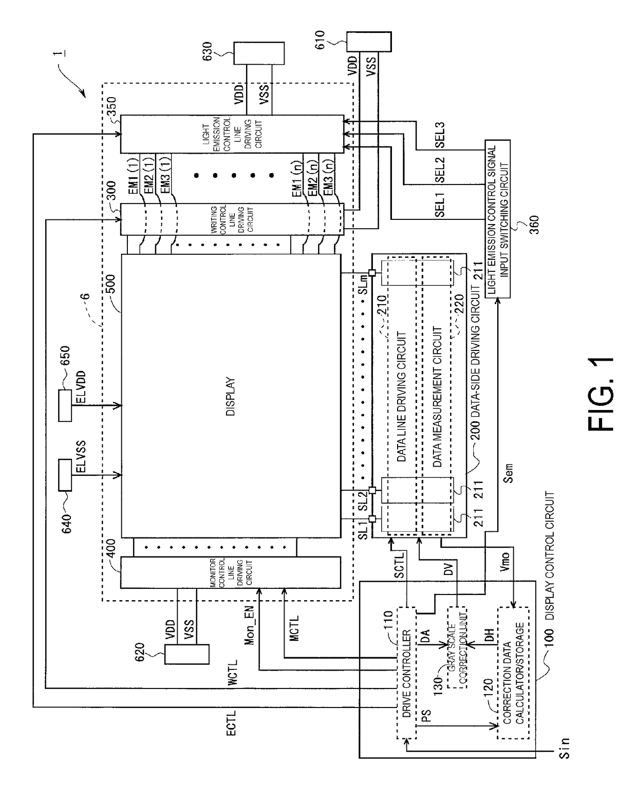
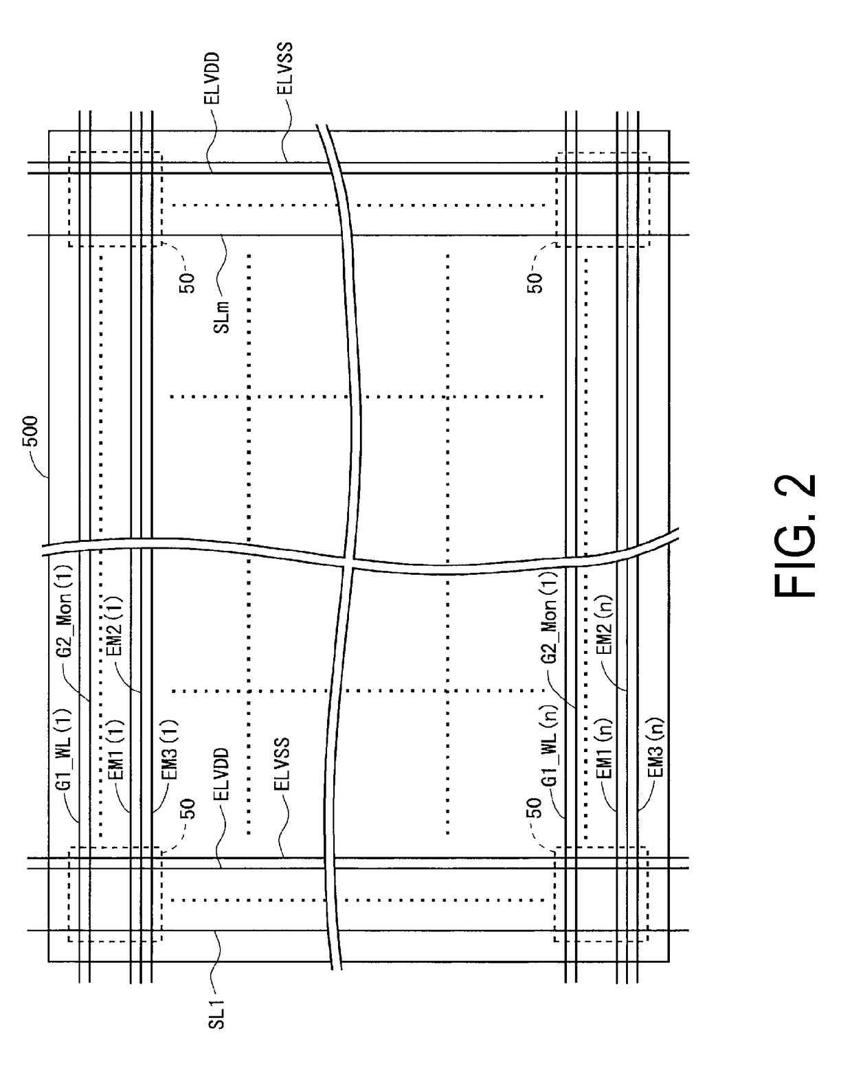
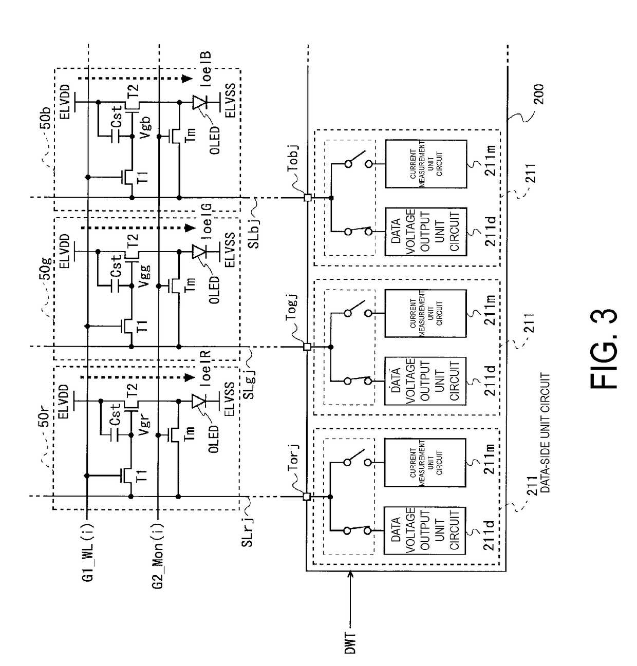
[0130]FIG. 1 is a block diagram illustrating an overall configuration of an active-matrix organic EL display device 1 according to a first embodiment of the present invention. The organic EL display device 1 is a display device configured to display color images in a field sequential method and includes a display control circuit 100, a data-side driving circuit 200, a writing control line driving circuit 300, a monitor control line driving circuit 400, a light emission control line driving circuit 350, a light emission control signal input switching circuit 360, and a display 500. The data-side driving circuit 200 functionally includes a data line driving circuit 210 and a current measurement circuit 220. Note that, the writing control line driving circuit 300, the monitor control line driving circuit 400, and the light emission control line driving circuit 350 are formed integrally with the display device 500 in an org...

second embodiment

2. Second Embodiment

[0296]Next, a description will be given of an active-matrix organic EL display device according to a second embodiment of the present invention.

[0297]As has been described, in the above-described first embodiment, the mode control signal Cm indicates, for each frame period, whether to act in the normal display mode or act in the current measurement mode. The organic EL display device according to the above-described first embodiment acts as illustrated in FIG. 25 in the frame period for which the mode control signal Cm indicates the normal display mode while acting as illustrated in FIG. 29 and FIG. 32 in the frame period for which the mode control signal Cm indicates the current measurement mode. In the above-described first embodiment, the mode control signal Cm can specify any frame period to perform current measurement and correction data calculation.

[0298]In this configuration, for example, an action of displaying a color image in a field sequential method a...

third embodiment

3. Third Embodiment

[0304]Next, a description will be given of an active matrix organic EL display device according to a third embodiment of the present invention. In the present embodiment, the display device includes a configuration of acting in the current measurement mode in a period where the display device is turned on but is not used (referred to as a “DP disuse period” below). With this configuration, as illustrated in FIG. 40, a DP disuse detection circuit 163 is provided in or outside the drive controller 110 in the display control circuit 100, the DP disuse detection circuit 163 being configured to detect a DP disuse period on the basis of the RGB video data signal Din included in the input signal Sin from an external unit and timing information such as the external clock signal CLKin. A DP disuse signal Sdpn indicating whether the display device is used is output from the DP disuse detection circuit 163, and the DP disuse signal Sdpn is input to the status machine 115 in ...


PUM


Abstract

In each of pixel circuits in an organic EL display device configured to display color images in a field sequential method, a drive transistor is connected to first to third organic EL elements configured to emit red light, green light, and blue light through first to third light emission control transistors. A connection point between the drive transistor and the light emission control transistors is connected to a data line through a monitor control transistors. A data-side driving circuit is provided with a data voltage output unit circuit and a current measurement unit circuit for each of data lines. The data-side driving circuit is configured to be able to switch between the unit circuits to connect either one of the unit circuits to the data line.

Description

TECHNICAL FIELD[0001]The present disclosure relates to an active matrix display device and, more specifically, relates to an active matrix display device including a current-driven self-luminescent display elements, such as an organic EL display device, and a driving method therefor, and a pixel circuit in such a display device.BACKGROUND ART[0002]As display elements included in display devices, there have been known electrooptical elements in each of which luminescence is controlled using voltage applied to the electrooptical element and electrooptical elements in each of which luminescence is controlled using current passing through the electrooptical element. A representative example of the electrooptical element in which luminance is controlled using voltage applied to the electrooptical element is a liquid crystal display element. Meanwhile, a representative example of the electrooptical element in which luminance is controlled using current passing through the electrooptical e...

Claims


Application Information

Patent Timeline
Patent Type & Authority Applications(United States)
IPC IPC(8): G09G3/20H01L27/32G09G3/3258G09G3/3233
CPCG09G3/2003H01L27/3276G09G2310/0264G09G3/3233G09G3/3258G09G3/3266G09G2300/0465G09G2310/0291G09G2310/0294G09G2310/0297G09G2320/0223G09G2320/0295G09G2320/045H10K59/131
Inventor OHARA, MASANORIUCHIDA, HIDEKIKIKUCHI, KATSUHIROTSUKAMOTO, YUTOKOIKE, EIJITAKIZAWA, KAZUONOGUCHI, NOBORUKISHI, NORITAKAITO, ASAEISOMURA, YOSHIYUKI
Owner SHARP KK
Why Eureka
Try Eureka