Input/output devices with robustness of ESD protection

a technology of esd protection and input/output devices, which is applied in the direction of overvoltage protection resistors, emergency protection arrangements for limiting excess voltage/current, and arrangements responsive to excess voltage, etc., can solve the problem of inefficient esd protection schemes, i/o circuits may be problematic, and ic products are damaged by esd (electrostatic discharge) damage, etc. problem, to achieve the effect of robustness of esd protection

Inactive Publication Date: 2006-06-01
TAIWAN SEMICON MFG CO LTD
View PDF10 Cites 16 Cited by
  • Summary
  • Abstract
  • Description
  • Claims
  • Application Information

AI Technical Summary

Benefits of technology

[0008] An embodiment of the invention provides an input / output device with robustness of ESD protection. The input / output device comprises an input / output pad, a first NMOS transistor, a second NMOS transistor and an ESD detector. The first NMOS transistor comprises a first drain, a first source and a first gate, wherein the first source and the first gate are coupled to a first ground power rail, and the first drain to the input / output pad. The second NMOS transistor comprises a second drain, a second source and a second gate, wherein the second source is coupled to the first ground power rail, the second drain to the input / output pad, and the second gate to a first pre-driver. When an ESD event is detected, the ESD detector makes the first pre-driver couple the second gate to the first ground power rail, thereby the first and second transistors evenly discharge ESD current.

Problems solved by technology

ESD (electrostatic discharge) damage to IC products has become an essential reliability issue among others.
The I / O circuit may be problematic in view of ESD protection.
It implies that even though a finger-type NMOS transistor is used for ESD protection, this scheme of ESD protection is inefficient because not all BJTs in the finger-type NMOS transistor participate at the same time to discharge ESD current.

Method used


Image

  • Input/output devices with robustness of ESD protection
  • Input/output devices with robustness of ESD protection
  • Input/output devices with robustness of ESD protection

Examples


Embodiment Construction

[0021] The following description is of the best-contemplated mode of carrying out the invention. This description is made for the purpose of illustrating the general principles of the invention and should not be taken in a limiting sense. The scope of the invention is best determined by reference to the appended claims.

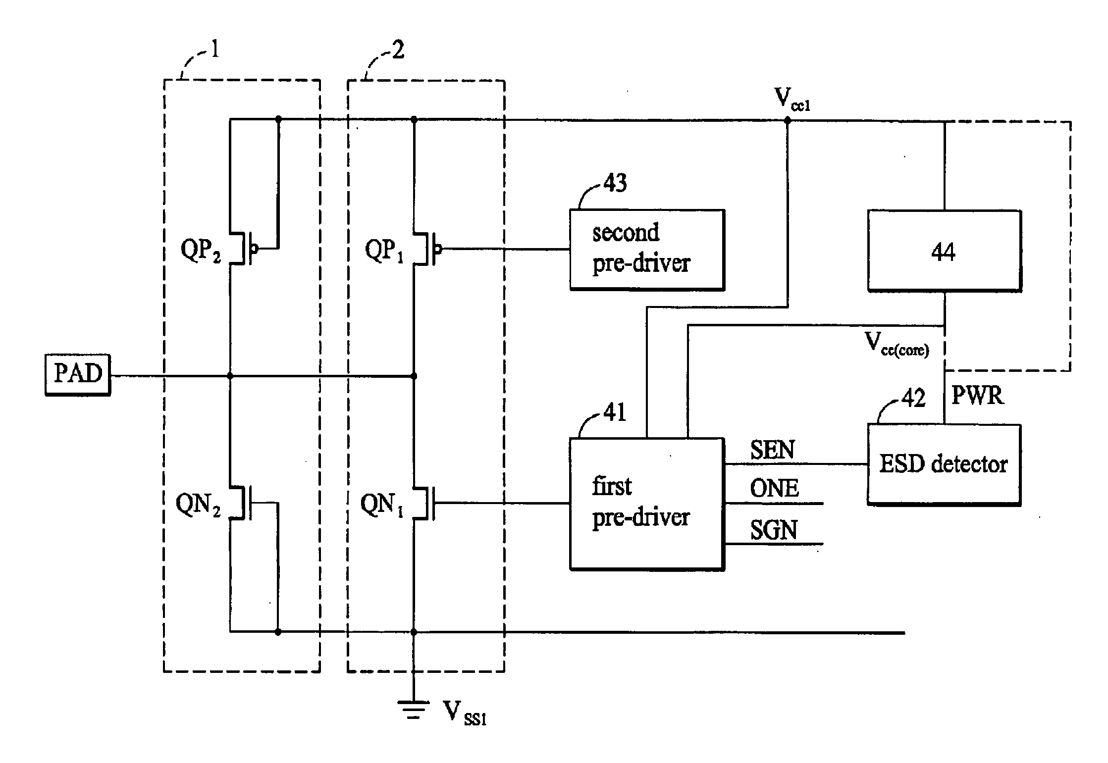
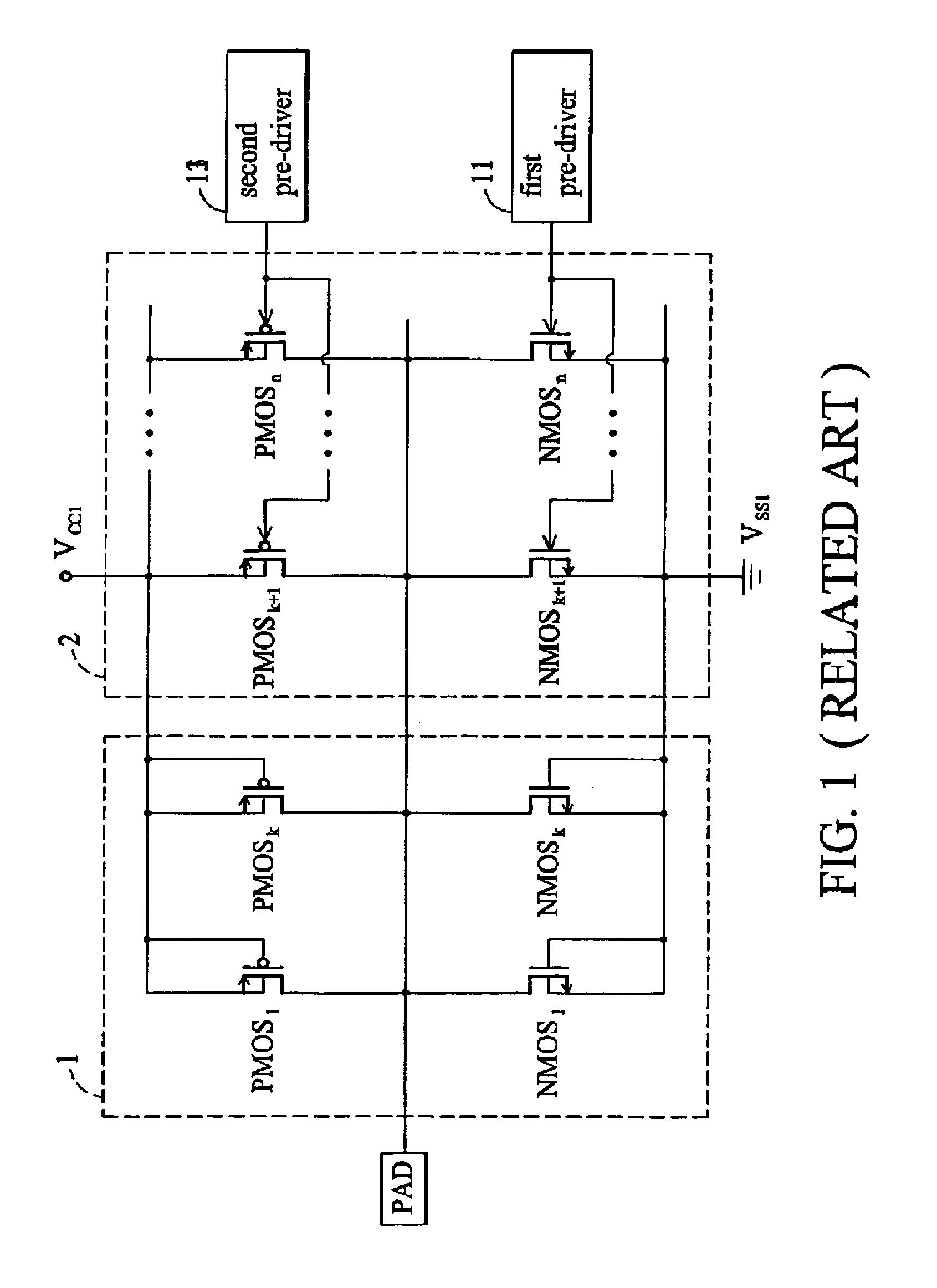
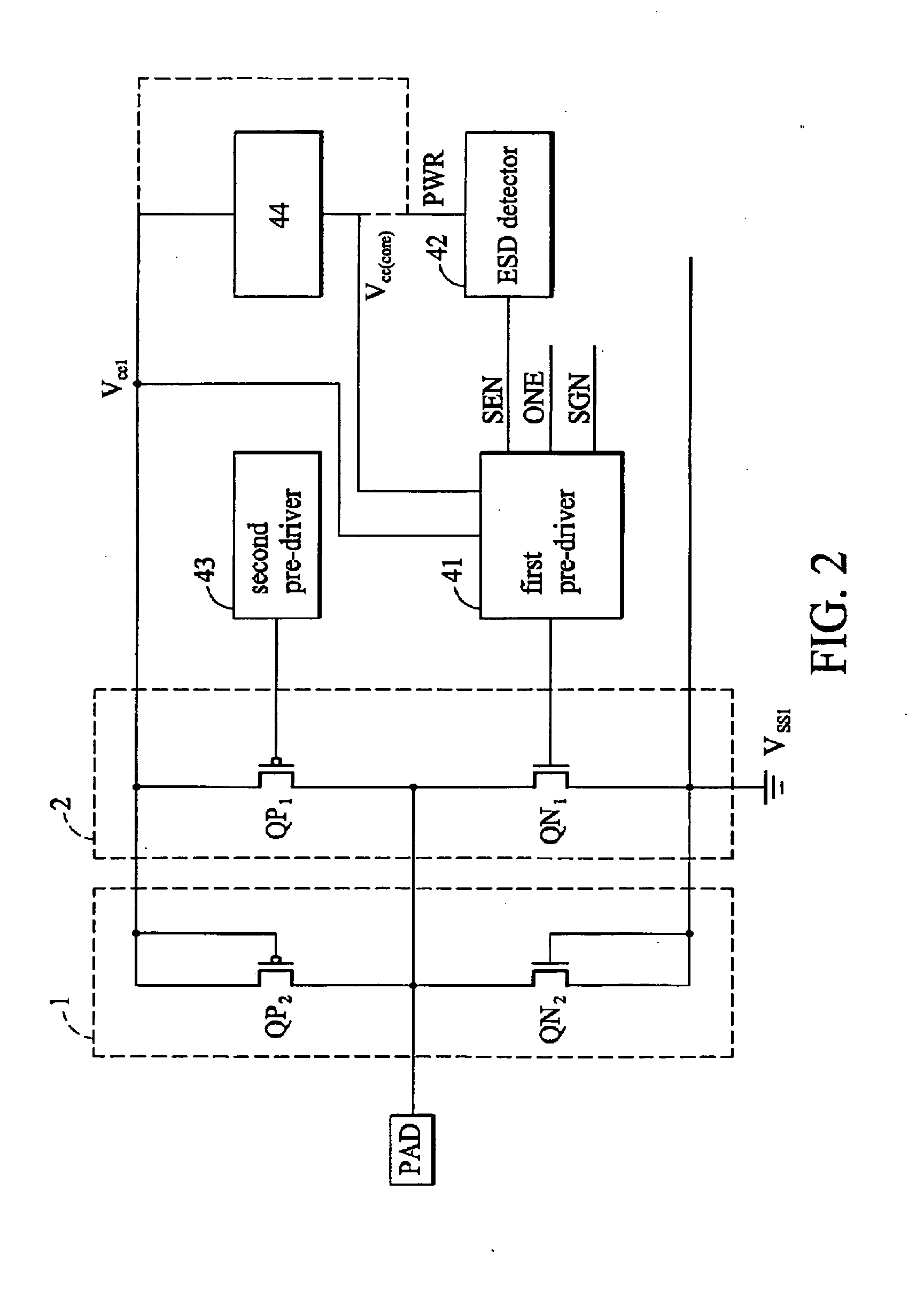
[0022]FIG. 2 shows an I / O circuit according to embodiments of the invention. The post driver in an I / O circuit can comprise a used part 2 and a non-used part 1. For clarity, only a NMOS transistor and a PMOS transistor are shown in the used part 2, and only another NMOS transistor and another PMOS transistor in the non-used part 1. The NMOS transistors may belong to a finger-type NMOS transistor, and the PMOS transistors may belong to a finger-type PMOS transistor. It can be understood by a person skilled in the art that the number of transistors in the used or non-used part is merely exemplary and can be less or more than 2.

[0023] The I / O circuit in FIG. 2 comprise...


PUM


Abstract

Input/output devices with robustness of ESD protection are provided. An input/output device comprises an input/output pad, a first NMOS transistor, a second NMOS transistor and an ESD detector. The first NMOS transistor comprises a first drain, a first source and a first gate, wherein the first source and the first gate are coupled to a first ground power rail, and the first drain to the input/output pad. The second NMOS transistor comprises a second drain, a second source and a second gate, wherein the second source is coupled to the first ground power rail, the second drain to the input/output pad, and the second gate to a first pre-driver. When an ESD event is detected, the ESD detector makes the first pre-driver couple the second gate to the first ground power rail, thereby the first and second transistors evenly discharge ESD current.

Description

CROSS REFERENCE TO RELATED APPILCATIONS [0001] This application is a continuation-in-part of pending U.S. patent application Ser. No. 10 / 307,646, filed Dec. 2, 2002 and entitled “Scheme for eliminating the channel unexpected turn-on during ESD zapping”, whose content as a whole is incorporated by reference in this application.BACKGROUND OF THE INVENTION [0002] 1. Field of the Invention [0003] The invention relates to input / output devices for ESD protection in an integrated circuit, and in particular to input / output devices that evenly discharge ESD current during an ESD event. [0004] 2. Description of the Related Art [0005] ESD (electrostatic discharge) damage to IC products has become an essential reliability issue among others. As feature size is scaled down to deep sub-micro, the gate oxide of a MOS transistor becomes thinner to render ICs more vulnerable to ESD stress. Industrial standards require input / output (I / O) pins to pass ESD tests of 2000 volts of human body mode (HBM) a...

Claims


Application Information

Patent Timeline
Patent Type & Authority Applications(United States)
IPC IPC(8): H02H9/00H01L27/02
CPCH01L27/0266H01L2924/0002H01L2924/00
Inventor WU, YI-HSUNLEE, JIAN-HSINGCHEN, SHUI-HUNG
Owner TAIWAN SEMICON MFG CO LTD
Why Eureka
Try Eureka