
Memory module having interconnected and stacked integrated circuits

a memory module and integrated circuit technology, applied in the direction of solid-state devices, basic electric elements, instruments, etc., can solve the problems of increasing the overall cost of the package, affecting the overall efficiency of the package,

Inactive Publication Date: 2006-06-08
SANDISK TECH LLC
View PDF99 Cites 32 Cited by
  • Summary
  • Abstract
  • Description
  • Claims
  • Application Information

AI Technical Summary

Benefits of technology

The present invention provides a multi-chip memory subsystem that can be used in a memory card without the need for expensive and time-consuming packaging. The subsystem includes stacked integrated circuits that are bonded together and have conductors that extend in a single row near the edge of the memory module. The conductors can be connected to a memory card package and can be used to transfer signals to and from the integrated circuits. The subsystem can be easily inserted and removed from the memory card receptor. The invention also includes a lead frame structure that allows for the stacking of integrated circuits and the formation of a memory module on a lead frame. The first integrated circuit can be a memory chip, while the second integrated circuit can be a controller. The second portion of the lead frame includes a plurality of conductors that can be used for frictional engagement with conductive elements in the receptor. The invention also includes a power and ground planar element that allows for separate power and ground connections.

Problems solved by technology

However, the side-by-side MCM may suffer from low package efficiency since the area of the package substrate generally increases with an increase in the number of integrated circuits mounted on the package substrate.
Such an increase in package size may also increase the overall cost of the package.
The dummy bonding pads may be necessary only for mechanical and assembly reasons, and may not serve to communicate with internal circuitry of the integrated circuit.
However, this bonding arrangement may not be possible in other memory packaging configurations.
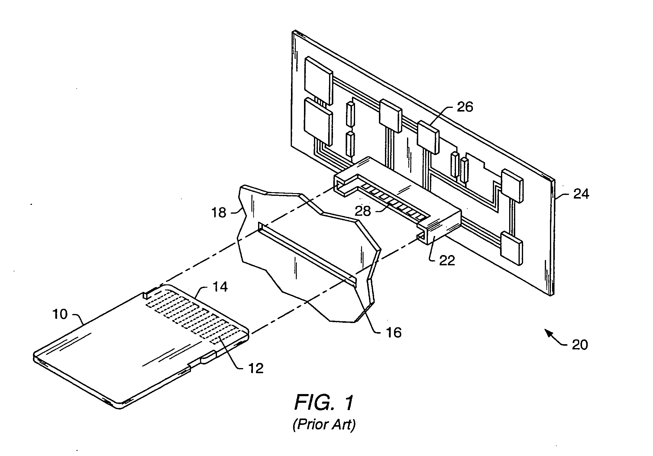
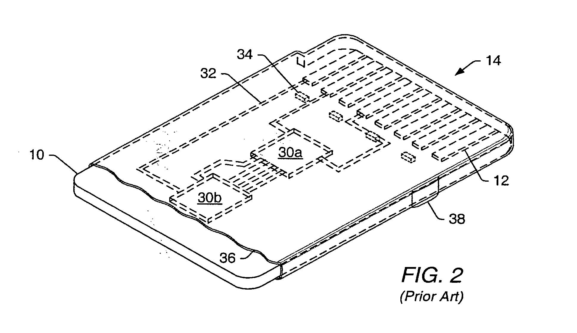
For example, the above bonding arrangement may not be possible in memory card configurations, since memory card edge connectors (i.e. bonding pads) may be arranged along only one side of the card.

Method used


Image

  • Memory module having interconnected and stacked integrated circuits
  • Memory module having interconnected and stacked integrated circuits
  • Memory module having interconnected and stacked integrated circuits

Examples


first embodiment

[0067]FIG. 6 illustrates the multi-chip module of the present invention in which stacked integrated circuits 40 may be incorporated onto substrate 62. Stacked integrated circuits 40 may include controller 40a and storage element 40b, such that controller 40a may be stacked upon and bonded to storage element 40b. In one example, controller 40a may also be electrically coupled to storage element 40b through a wire bonding process (i.e. wire bond 68). However, controller 40a may be coupled to storage element 40b by another bonding process, such as tape automated bonding (TAB) or flip-chip attachment. Preferably, storage element 40b may be a three-dimensional memory array, as described above.

[0068] Memory module 60 of FIG. 6 may also include a first set of wires 69 extending between controller 40a and trace conductors 64. Trace conductors 64 may be arranged on the surface of substrate 62 and / or embedded within the thickness of substrate 62. Trace conductors 64 may, therefore, include on...

second embodiment

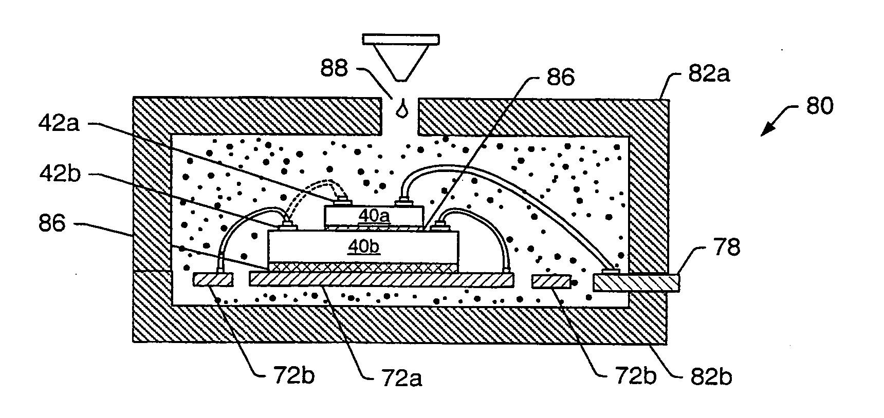
[0070]FIG. 7 illustrates the multi-chip module of the present invention in which stacked integrated circuits 40 may be incorporated onto lead frame 70. In one example, first integrated circuit 40b may be a three-dimensional memory array, as described above. However, the scope of the present invention may include any storage element, or any other integrated circuit. Lead frame 70 may contain a first portion 72 (i.e. paddle) that may be configured below stacked integrated circuits 40. Integrated circuits 40 may be bonded to the first portion of lead frame using, for example, a die attach adhesive. The die attach adhesive may be tape or epoxy based. As such, lead frame 70 may serve to support the molded memory module, and thus, may be fabricated from a strip of sheet metal by stamping or chemical milling. Lead frame 70 may also provide a holding fixture during the assembly process in which bonding pads 42 of integrated circuits 40 may be connected to the lead frame. After molding, lead...


PUM


Abstract

A multi-chip memory module may be formed including two or more stacked integrated circuits mounted to a substrate or lead frame structure. The memory module may include means to couple one or more of the stacked integrated circuits to edge conductors in a memory card package configuration. Such means may include the capability to utilize bonding pads on all four sides of an integrated circuit. A lead frame structure may be divided into first and second portions. The first portion may be adapted to receive the stacked integrated circuits and the second portion may include a plurality of conductors. The first portion may also be adapted to couple at least one of the integrated circuits to power and ground conductors on the second portion. In one embodiment, the first portion may include the lead frame paddle and a conductive ring. In another embodiment, the first portion may include first and second coplanar elements.

Description

CROSS REFERENCE TO RELATED APPLICATIONS [0001] This application is related to commonly assigned: [0002] U.S. Pat. Nos. 6,034,882 and 6,185,122, both titled “Vertically Stacked Field Programmable Nonvolatile Memory and Method of Fabrication”, by inventor Mark G. Johnson et al.; [0003] U.S. patent application Ser. No. 09 / 814,727 and Ser. No. 09 / 560,626, both titled “Three Dimensional Memory Array and Method of Fabrication”, by Johan Knall et al, filed Apr. 21, 2001 and Apr. 28, 2000, respectively; [0004] U.S. patent application Ser. No. 09 / 928,536 titled “Vertically Stacked, Field Programmable, Nonvolatile-Memory and Method of Fabrication” by Mark G. Johnson, filed Aug. 13, 2001; [0005] U.S. patent application Ser. No. 10 / 010,643, titled “Insulator Programmed Mask ROM Memory Cells for a 3-Dimensional Memory Array”, by Mark G. Johnson, filed Nov. 5, 2001; [0006] all of which are incorporated herein by reference.BACKGROUND OF THE INVENTION [0007] 1. Field of the Invention [0008] This in...

Claims


Application Information

Patent Timeline
Patent Type & Authority Applications(United States)
IPC IPC(8): H01L23/495G06K19/077H01L23/538H01L25/065
CPCG06K19/072G06K19/07745H01L23/3107H01L23/49537H01L23/49551H01L23/49575H01L23/5388H01L24/45H01L24/49H01L25/0657H01L25/18H01L27/0688H01L27/112H01L2224/32145H01L2224/45124H01L2224/48091H01L2224/48145H01L2224/48247H01L2224/48257H01L2224/49171H01L2225/06506H01L2225/0651H01L2225/06555H01L2225/06562H01L2225/06579H01L2225/06582H01L2924/01013H01L2924/01014H01L2924/01015H01L2924/01028H01L2924/01029H01L2924/01079H01L2924/01082H01L2924/01322H01L2924/14H01L2924/19041H01L24/48H01L2224/32245H01L2224/73265H01L2924/01033H01L2924/12032H01L2924/00014H01L2924/00H01L2924/181H10B20/00H01L2924/00012
Inventor VERMA, VANICHHOR, KHUSHRAV S.
Owner SANDISK TECH LLC
Learn More