Piezoelectric/electrostrictive device and method for manufacturing the same

a piezoelectric/electrostrictive and electrode technology, applied in the field of piezoelectric/electrostrictive devices, can solve problems such as cracks achieve superior piezoelectric/electrostrictive characteristics, reduce residual stress in the piezoelectric/electrostrictive layer, and prevent degradation of the piezoelectric/electrostrictive layer resulting from residual stress

Inactive Publication Date: 2006-06-08
NGK INSULATORS LTD
View PDF7 Cites 23 Cited by
  • Summary
  • Abstract
  • Description
  • Claims
  • Application Information

AI Technical Summary

Benefits of technology

[0013] By cooling the piezoelectric / electrostrictive device after the firing step (at a temperature decreasing rate of at least the natural cooling rate), the grain size of the piezoelectric / electrostrictive layer is controlled to exhibit desired piezoelectric / electrostrictive characteristics. Specifically, the excessive growth of the crystal grains in the piezoelectric / electrostrictive layer, which is caused by simple natural cooling, can be prevented. By holding the piezoelectric / electrostrictive device at a predetermined holding temperature, high-temperature creep occurs in the metal-based electrode layer by the residual stress produced in the piezoelectric / electrostrictive layer during cooling by the difference in thermal expansion coefficient between the substrate and the piezoelectric / electrostrictive layer. Hereby, the residual stress is reduced by the high-temperature creep.
[0018] According to the present invention, the residual stress in the piezoelectric / electrostrictive layer can be reduced by (high-temperature) creep. Consequently, the degradation of the characteristics of the piezoelectric / electrostrictive layer resulting from the residual stress can be prevented, and the resulting piezoelectric / electrostrictive device can exhibit superior piezoelectric / electrostrictive characteristics.

Problems solved by technology

In addition, the piezoelectric / electrostrictive layer may be cracked during the cooling step or a subsequent polarization step.

Method used


Image

  • Piezoelectric/electrostrictive device and method for manufacturing the same
  • Piezoelectric/electrostrictive device and method for manufacturing the same
  • Piezoelectric/electrostrictive device and method for manufacturing the same

Examples


examples

[0057] Examples for confirming the effect of the above-described embodiment will now be described. The Examples evaluated the piezoelectric / electrostrictive characteristics of a piezoelectric / electrostrictive device 10″ shown in FIG. 4, prepared by a process in which the conditions of the cooling step and applied voltage (hereinafter referred to as polarization voltage) for polarization of the piezoelectric / electrostrictive layer 13 were varied.

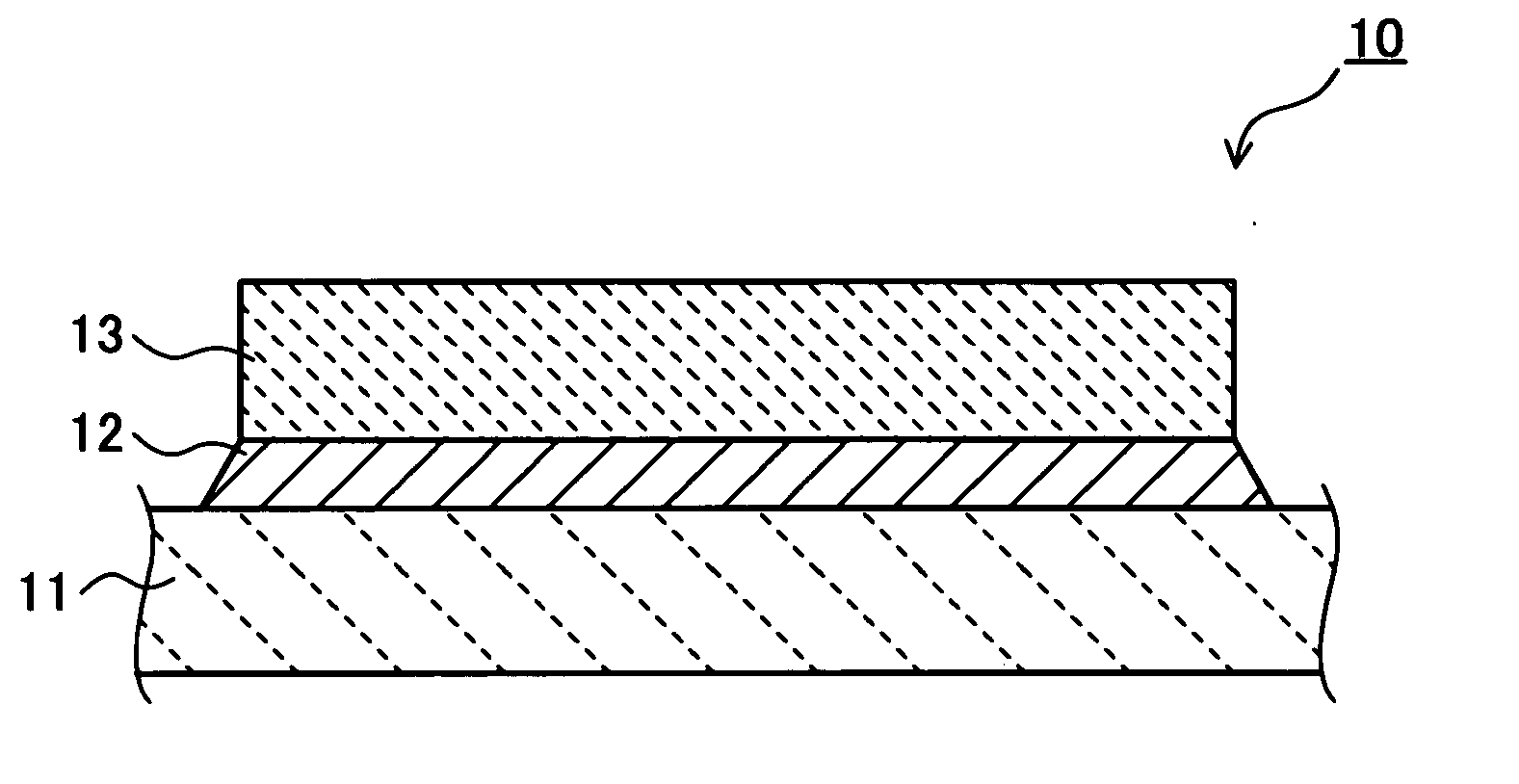
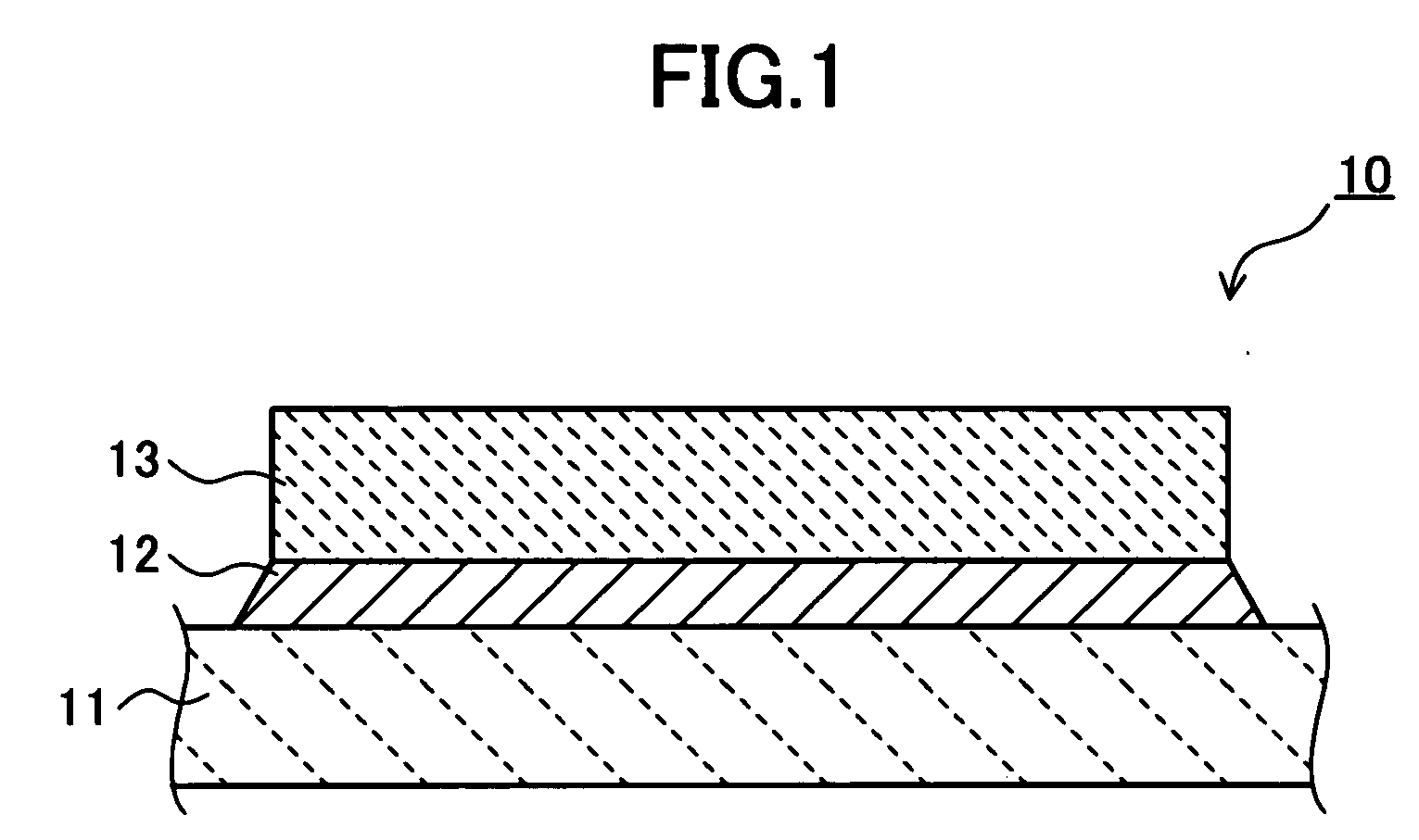
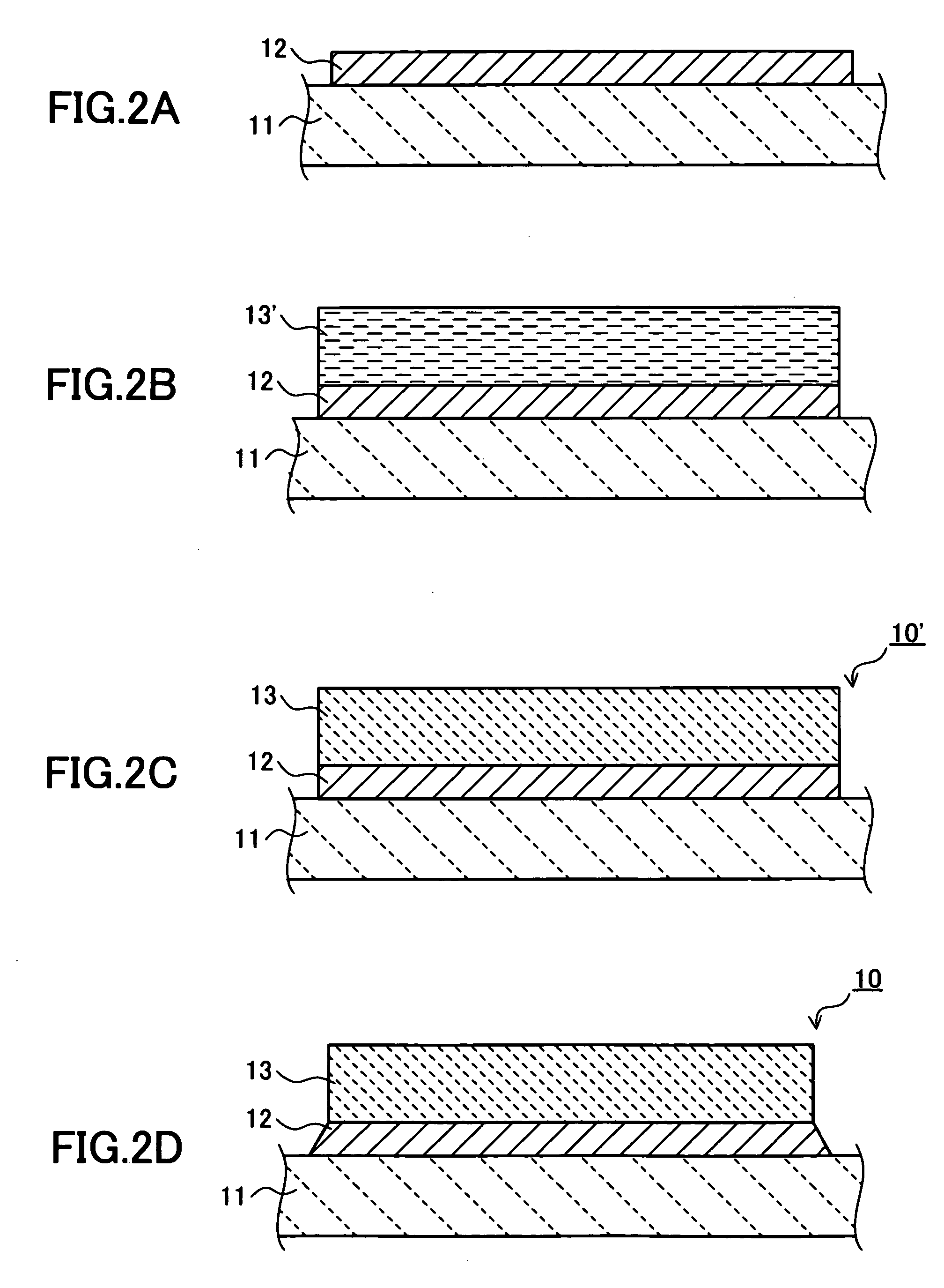
[0058] The piezoelectric / electrostrictive device 10″ had the following structure. The piezoelectric / electrostrictive device 10″ included the intermediate electrode layer 12 and the piezoelectric / electrostrictive layer 13 on a vibration plate 11a corresponding to the substrate 11 shown in FIGS. 1 and 2A to 2D. In addition, an upper electrode 14 was formed on the piezoelectric / electrostrictive layer 13.

[0059] In the piezoelectric / electrostrictive device 10″, a polarization voltage was applied between intermediate electrode layer 12 and the up...


PUM

PropertyMeasurementUnit
thicknessaaaaaaaaaa
thicknessaaaaaaaaaa
thicknessaaaaaaaaaa

Abstract

A piezoelectric / electrostrictive device includes a substrate, an electrode layer adhering to the surface of the substrate, and a piezoelectric / electrostrictive layer adhering to the electrode layer. The electrode layer is deformed by high-temperature creep. A method for manufacturing the piezoelectric / electrostrictive device includes the cooling step of cooling the piezoelectric / electrostrictive device after firing at a temperature decreasing rate of at least the rate of natural cooling. The cooling step includes the sub-step of holding the piezoelectric / electrostrictive device at a constant temperature lower than the firing temperature. The holding temperature is set within the range of temperatures at which high-temperature creep occurs in the metal of the electrode layer. Thus, residual stress in the piezoelectric / electrostrictive layer can be reduced.

Description

BACKGROUND OF THE INVENTION [0001] 1. Field of the Invention [0002] The present invention relates to a piezoelectric / electrostrictive device including an electrode layer adhering to the upper surface of a substrate and a piezoelectric / electrostrictive layer adhering to the upper surface of the electrode layer, and to a method for manufacturing the same. [0003] 2. Description of the Related Art [0004] A piezoelectric / electrostrictive device having such a structure has been disclosed in, for example, Japanese Unexamined Patent Application Publication No. 2001-284677. The piezoelectric / electrostrictive device has a metal-based electrode layer in tight contact with the surface of a ceramic substrate mainly containing zirconia, and piezoelectric / electrostrictive layer in tight contact with the electrode layer. The piezoelectric / electrostrictive device having such a structure is generally manufactured by the following process. [0005] First, an electrode layer or an electrode precursor coa...

Claims


Application Information

Patent Timeline
Patent Type & Authority Applications(United States)
IPC IPC(8): H01L41/18H01L41/09H01L41/187H01L41/22H01L41/43
CPCH01L41/43Y10T29/42H01L41/314H01L41/0973H10N30/2047H10N30/074H10N30/097
Inventor KOIZUMI, TAKAAKIYAMAGUCHI, HIROFUMI
Owner NGK INSULATORS LTD
Why Eureka
Try Eureka