Semiconductor device

a semiconductor device and semiconductor technology, applied in the direction of semiconductor devices, semiconductor/solid-state device details, instruments, etc., can solve the problems of insufficient lowering of the wiring resistance of the source wiring, inability to efficiently wire singal wirings, and increase in operation delay and erroneous operation of the circuit element, so as to achieve the effect of more wiring resources for signal wiring

Active Publication Date: 2006-06-22
PANASONIC SEMICON SOLUTIONS CO LTD
View PDF3 Cites 4 Cited by
  • Summary
  • Abstract
  • Description
  • Claims
  • Application Information

AI Technical Summary

Benefits of technology

[0045] In the above structure, the third contact is formed at at least one of the intersections where the third source wirings and the fourth source wirings intersect with each other, ensuring more wiring resources for signal wiring.

Problems solved by technology

Otherwise, severe voltage drop occurs when a current flows in the source wiring at initiation of the operation of the circuit element, inviting increase in operation delay and erroneous operation of the circuit element.
However, the above conventional semiconductor device involves the following problems.
Namely, the contacts 660 for cell source wiring consume wiring resources (region required for wiring) in a plurality of wiring layers, which in turn inhibits efficient wiring of singal wirings.
However, mere widening the wiring width of the mesh source wiring 610 and the cell source wirings 650 in the generation of, for example, about 0.13 μm process attains insufficient lowering of the wiring resistance of the source wirings.
In this way, it is difficult to suppress voltage drop of the source voltage to be supplied to the circuit elements 670.
In miniaturized wirings, the upper limit of the wiring width is restricted for increasing a manufacturing yield, so that voltage drop of the source voltage is difficult to be sufficiently suppressed even if the widths of all source wirings are set large as far as possible.
This degrades the timing of the signal wirings and necessitates increase in area of the semiconductor device for supplementing the short of the wiring resources.
Furthermore, the timing degradation involves many design steps for countermeasures thereto, inviting increase in design period.
Also, the increase in area of the semiconductor device invites voltage drop of the source voltage caused due to increase in lengthy routed source wirings and increases in manufacturing cost because of a lowered yield of the semiconductor device.

Method used


Image

  • Semiconductor device
  • Semiconductor device
  • Semiconductor device

Examples


embodiment 1

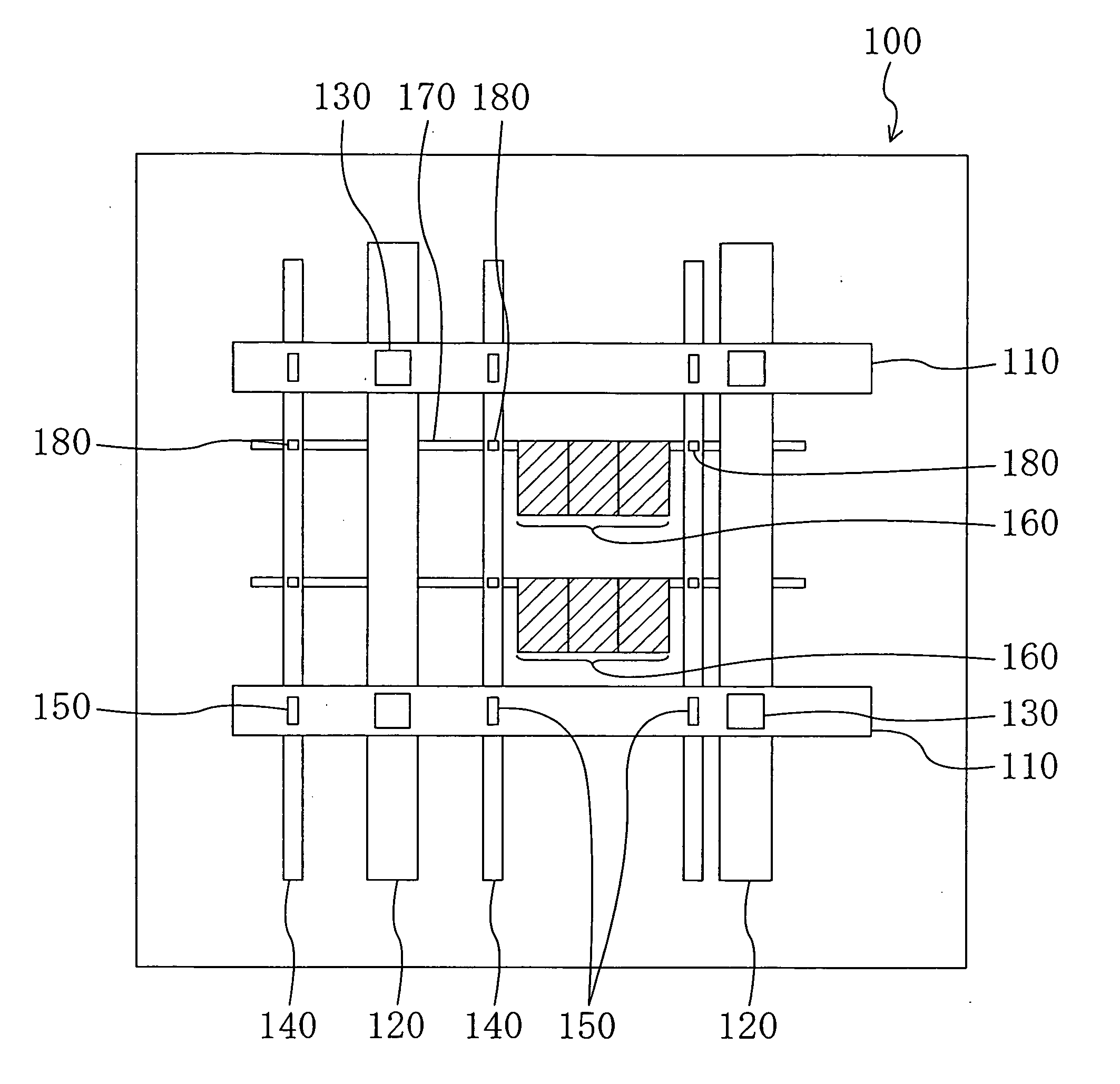
[0056]FIG. 1 is a plan view showing a construction of a semiconductor device 100 according to Embodiment 1 of the present invention.

[0057] The semiconductor device 100 has a plurality of wiring layers and includes, as shown in the drawing: a mesh-like source wiring (mesh source wiring) compose of a plurality of first source wirings 110, a plurality of second source wirings 120, and a plurality of contacts 130 for mesh source wiring; a plurality of strap source wirings 140; a plurality of contacts 150 for strap source wiring; a plurality of standard cells 160; a plurality of cell source wirings 170; and a plurality of contacts 180 for cell source wiring.

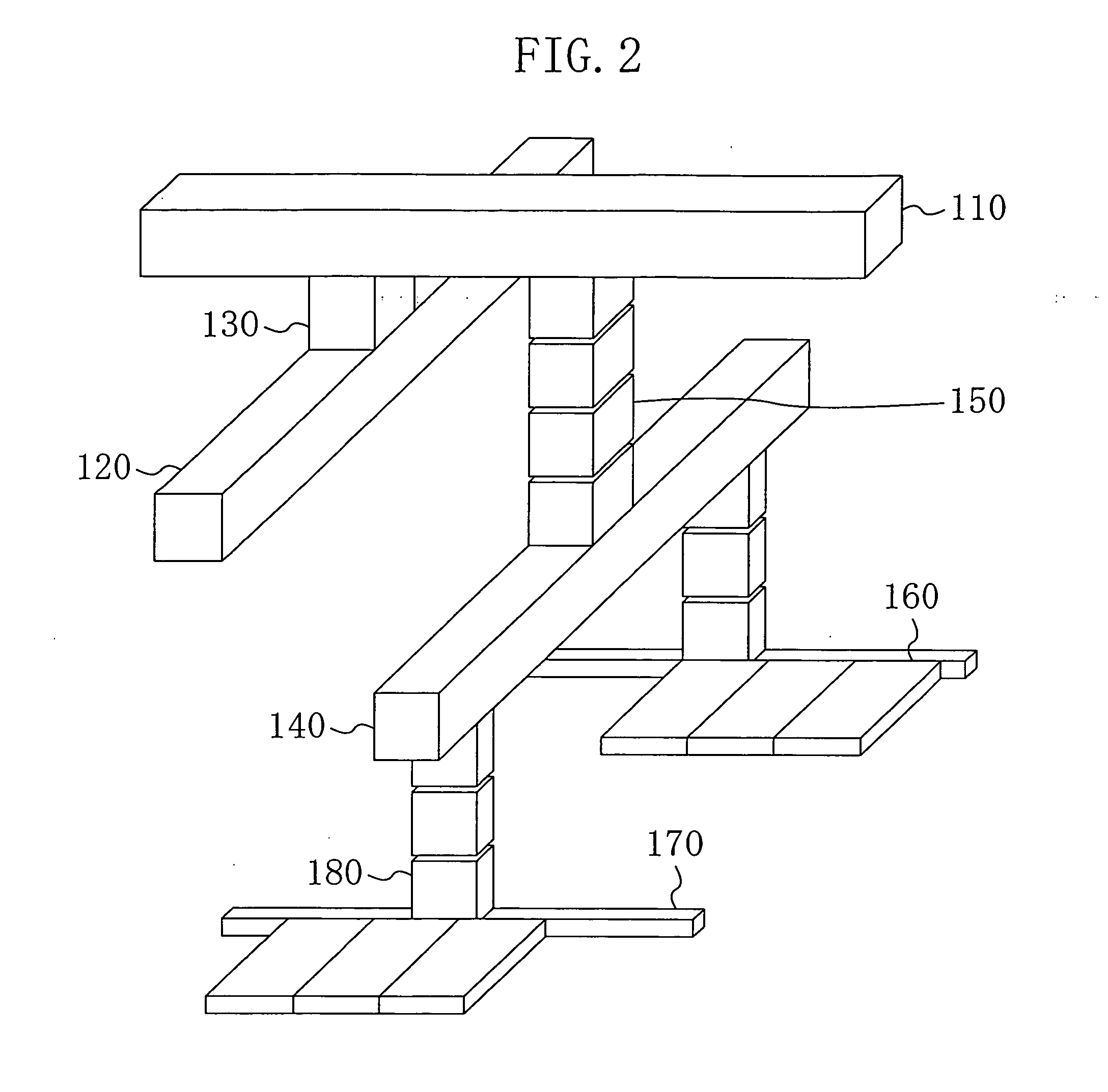
[0058]FIG. 2 is a drawing stereoscopically showing the positional relationship between the first source wirings 110 and the like. Wherein, in the following description, the wiring layer where the first source wirings 110 are formed is located on the upper side for the convenience sake.

[0059] The first source wirings 110 are formed,...

embodiment 2

[0074] An example is described in which the number of contacts for power supply is further reduced while the wiring resources are increased compared with Embodiment 1.

[0075] Wherein, in the following embodiments, the same reference numerals are assigned to the constitutional elements having the same functions as in Embodiment 1 and the description thereof is omitted.

[0076]FIG. 3 is a plan view showing a construction of a semiconductor device 200 according to Embodiment 2 of the present invention. FIG. 4 is a view stereoscopically showing the positional relationship of each constitutional element of the semiconductor device 200.

[0077] The semiconductor 200 is different from the semiconductor device in Embodiment 1, as shown in FIG. 3 and FIG. 4, in that the second source wirings 120 and the strap source wirings 140 are overlaid with each other when viewed from the wiring layer where the first source wirings 110 are formed and in that the contacts 130 for mesh source wiring and the...

embodiment 3

[0080]FIG. 5 is a plan view showing a construction of a semiconductor device 300 according to Embodiment 3 of the present invention.

[0081] In the semiconductor device 300, the strap source wirings 140 are formed so as to correspond to some of the second source wirings 120, different from the semiconductor device of Embodiment 2 in which the strap source wirings 140 are formed in one-to-one correspondence to the second source wirings 120. The number of the strap source wirings 140 formed is determined so that the value of voltage drop of the source voltage falls within a tolerable range.

[0082] With the above arrangement, the numbers of the contacts 150 for strap source wiring and the contacts 180 for cell source wiring can be further reduced compared with each of the above embodiments.

[0083] In addition, when the number of the strap source wirings 140 is determined as above, the number of the strap source wirings 140 can be reduced, increasing the wiring resources for a signal wir...


PUM


Abstract

A mesh source wiring composed of first source wirings, second source wirings, and contacts for mesh source wiring is connected, through contacts for strap source wiring, with strap source wirings formed on a wiring layer nearer a substrate than wiring layers where the mesh source wiring is formed. The cell source wirings formed on a wiring layer nearer the substrate than the wiring layer where the strap source wirings are formed are connected with the strap-source wirings through contacts for cell source wiring.

Description

CROSS REFERENCE TO RELATED APPLICATIONS [0001] This Non-provisional application claims priority under 35 U.S.C. §119(a) on Patent Application No. 2004-366609 filed in Japan on Dec. 17, 2004, the entire contents of which are hereby incorporated by reference. BACKGROUND OF THE INVENTION [0002] The present invention relates to a semiconductor device having a plurality of wiring layers, and more specifically relates to a wiring structure of a semiconductor device. [0003] Wiring resistance of a source wiring for supplying electric power to a circuit element in a semiconductor device must be set sufficiently small. Otherwise, severe voltage drop occurs when a current flows in the source wiring at initiation of the operation of the circuit element, inviting increase in operation delay and erroneous operation of the circuit element. In this connection, design of source wirings in semiconductor devices becomes a key in association with recent increase in scale and integration of semiconducto...

Claims


Application Information

Patent Timeline
Patent Type & Authority Applications(United States)
IPC IPC(8): H01L27/10
CPCH01L21/76838H01L23/5286H01L27/118H01L2924/0002H01L2924/00
Inventor KISHISHITA, KEISUKE
Owner PANASONIC SEMICON SOLUTIONS CO LTD
Why Eureka
Try Eureka