Electron emission display and a method of driving the electron emission display

Inactive Publication Date: 2006-06-29
SAMSUNG SDI CO LTD
View PDF6 Cites 4 Cited by
  • Summary
  • Abstract
  • Description
  • Claims
  • Application Information

AI Technical Summary

Benefits of technology

[0007] The present invention provides an electron emission display which enhances image reproducibility by efficiently compensating for brightness deviations due to the internal resistance of cathode electrode lines, and a method of driving the electron emission display.
[0022] By adjusting a reference voltage of the gate electrode lines, it is possible to efficiently compensate for brightness deviations due to the internal resistance of the cathode electrode lines. As a result, the reproducibility of images to be displayed is enhanced.
[0023] Preferably, an average reference voltage of the gate electrode lines in each frame is inversely proportional to an average gray-scale level of the each frame. Therefore, display quality in dark images as well as in bright images are efficiently improved.

Problems solved by technology

Accordingly, pixels disposed far from driving terminals for driving the cathode electrode lines used as data electrode lines have lowered brightness, which deteriorates image reproducibility.

Method used


Image

  • Electron emission display and a method of driving the electron emission display
  • Electron emission display and a method of driving the electron emission display
  • Electron emission display and a method of driving the electron emission display

Examples


Embodiment Construction

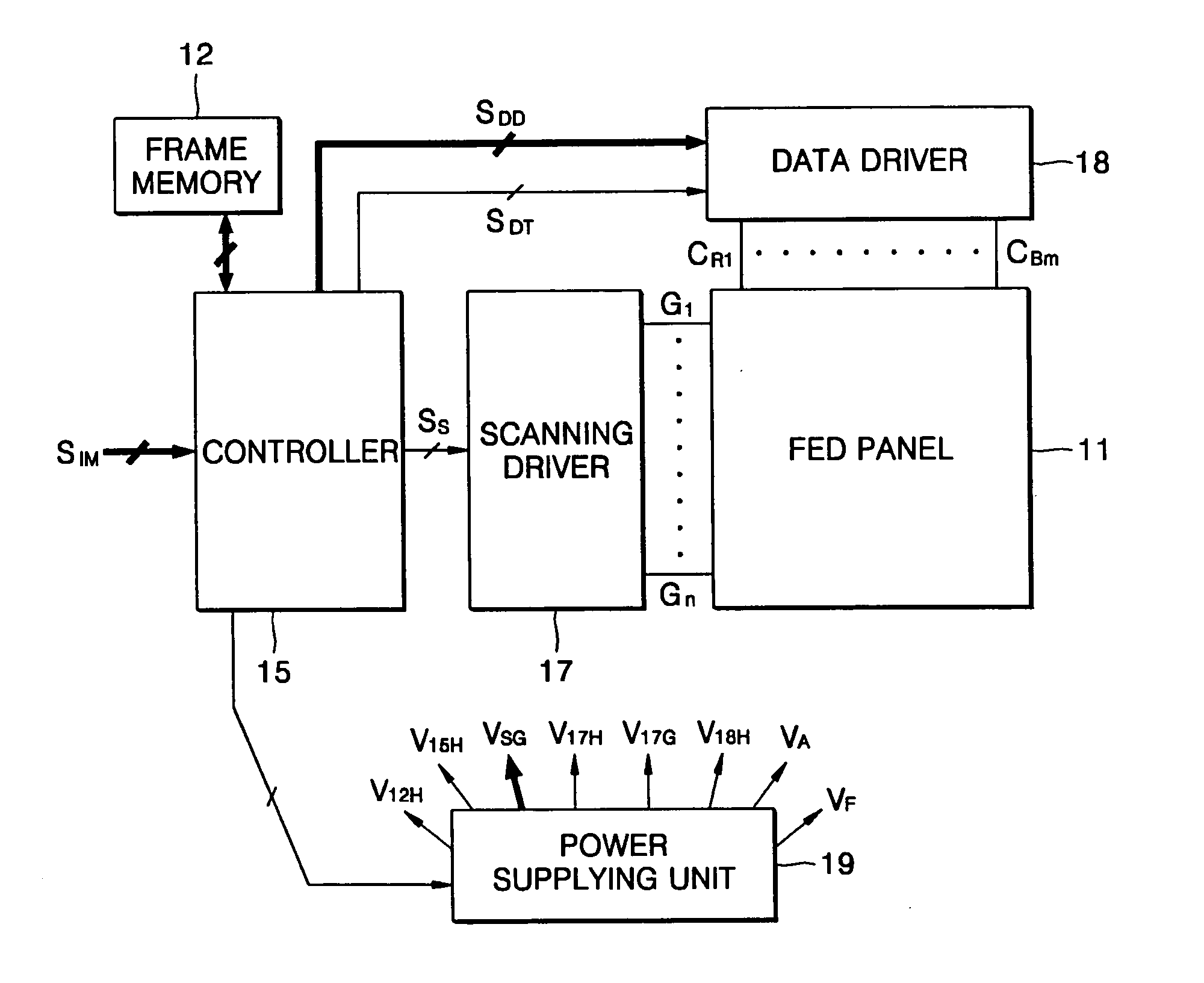
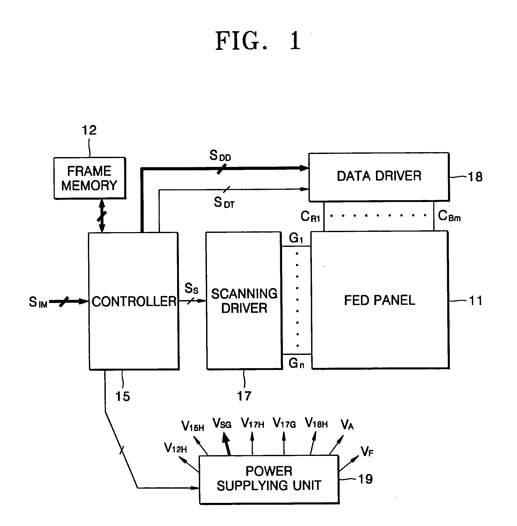
[0032]FIG. 1 is a block diagram of an electron emission display according to an embodiment of the present invention. FIG. 3 is a block diagram for explaining voltages which are supplied from a power supplying unit 19 of FIG. 1 to respective units.

[0033] Referring to FIGS. 1 and 3, the electron emission display includes an electron emission display panel 11 and a driving apparatus for driving the electron emission display panel 11. The driving apparatus includes a power supplying unit 19, a scanning driver 17, a data driver 18, a frame memory 12, and a controller 15.

[0034] The power supplying unit 19 supplies a system reference voltage VSG and an operating voltage V12H to the frame memory 12, supplies the system reference voltage VSG and an operating voltage V15H to the controller 15, supplies a variable reference voltage V17G and an operating voltage V17H to the scanning driver 17, supplies the system reference voltage VSG and an operating voltage V18H to the data driver 18, suppl...


PUM


Abstract

An electron emission display includes: cathode electrode lines electrically connected to electron emission sources; gate electrode lines including openings corresponding to the electron emission sources, the openings being arranged at intersections of the gate electrode lines and the cathode electrode lines; phosphor cells arranged to correspond to the openings of the gate electrode lines; and a positive plate adapted to receive a voltage and to move electrons emitted from the electron emission sources to the phosphor cells in accordance with the received voltage. Scanning pulses, having gradually rising voltages, are sequentially supplied to the gate electrode lines in a unit frame, such that reference voltages of the gate electrode lines gradually rise in proportion to relative distances between the gate electrode lines and driving terminals of the cathode electrode lines.

Description

CLAIM OF PRIORITY [0001] This application makes reference to, incorporates the same herein, and claims all benefits accruing under 35 U.S.C. §119 from an application for ELECTRON EMISSION DISPLAY APPARATUS WHEREIN REFERENCE ELECTRICAL POTENTIAL OF SCANNING ELECTRODE LINES VARIES earlier filled in the Korean Intellectual Property Office on 23 Dec. 2004 and there duly assigned Serial No. 10-2004-0111099. BACKGROUND OF THE INVENTION [0002] 1. Field of the Invention [0003] The present invention relates to an electron emission display and a method of driving the electron emission display, and, more particularly, to an electron emission display including cathode electrode lines, gate electrode lines, phosphor cells, and a positive plate, and a method of driving the electron emission display. [0004] 2. Description of the Related Art [0005] An electron emission display is discussed in U.S. Patent Publication No. 2003 / 0122118, entitled “FED Driving Method”, published on Jul. 3, 2003. The ele...

Claims


Application Information

Patent Timeline
IPC IPC(8): G09G3/22
CPCG09G3/2014G09G3/22G09G2310/0267G09G2320/0223G09G2320/0233G09G2320/0276G09G2330/02G09G2360/16
Inventor KANG, MUN-SEOK
Owner SAMSUNG SDI CO LTD
Why Eureka
Try Eureka