

High output light emitting diode and method for fabricating the same
a light-emitting diode, high-output technology, applied in the direction of basic electric elements, electrical appliances, semiconductor devices, etc., can solve the problems of wasting the light emitted from the sidewall of the device, reducing the light emission from the device, etc., to achieve high output and improve the effect of light outpu
- Summary
- Abstract
- Description
- Claims
- Application Information
AI Technical Summary
Benefits of technology
Problems solved by technology
Method used
Image

Examples
first embodiment
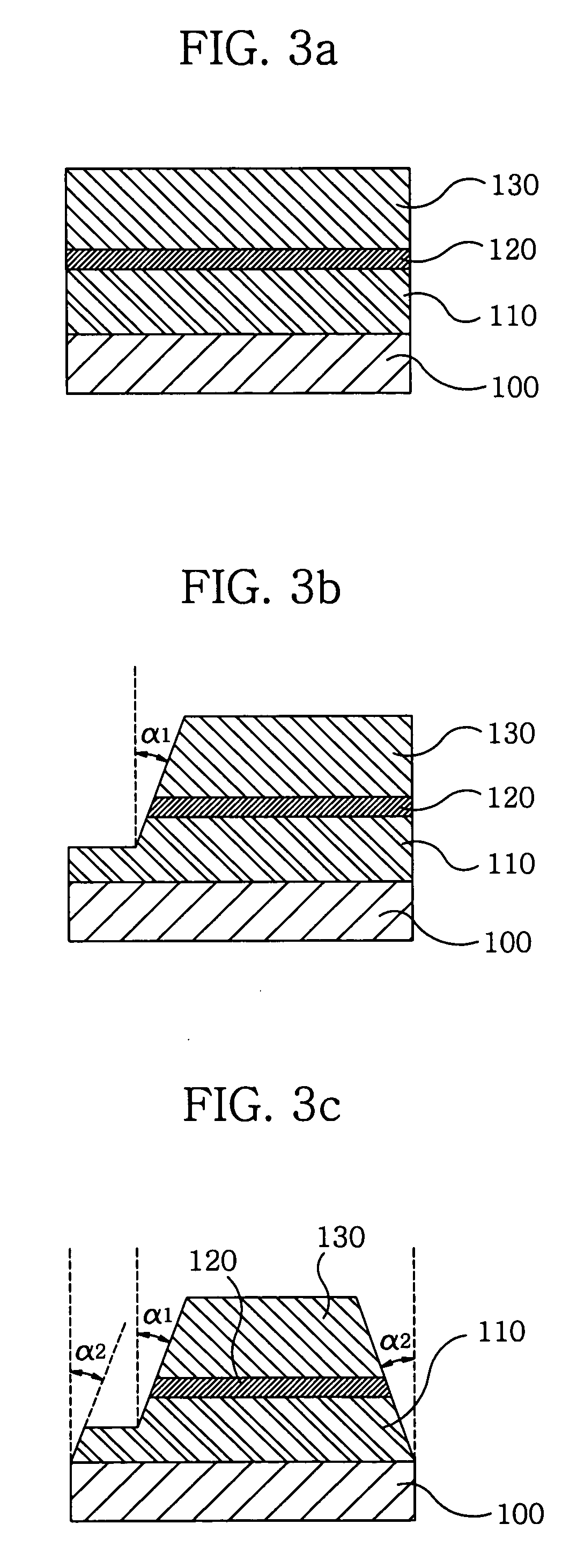
[0033]FIGS. 3a through 3e are cross-sectional views explaining a fabricating process of a high output LED according to the present.
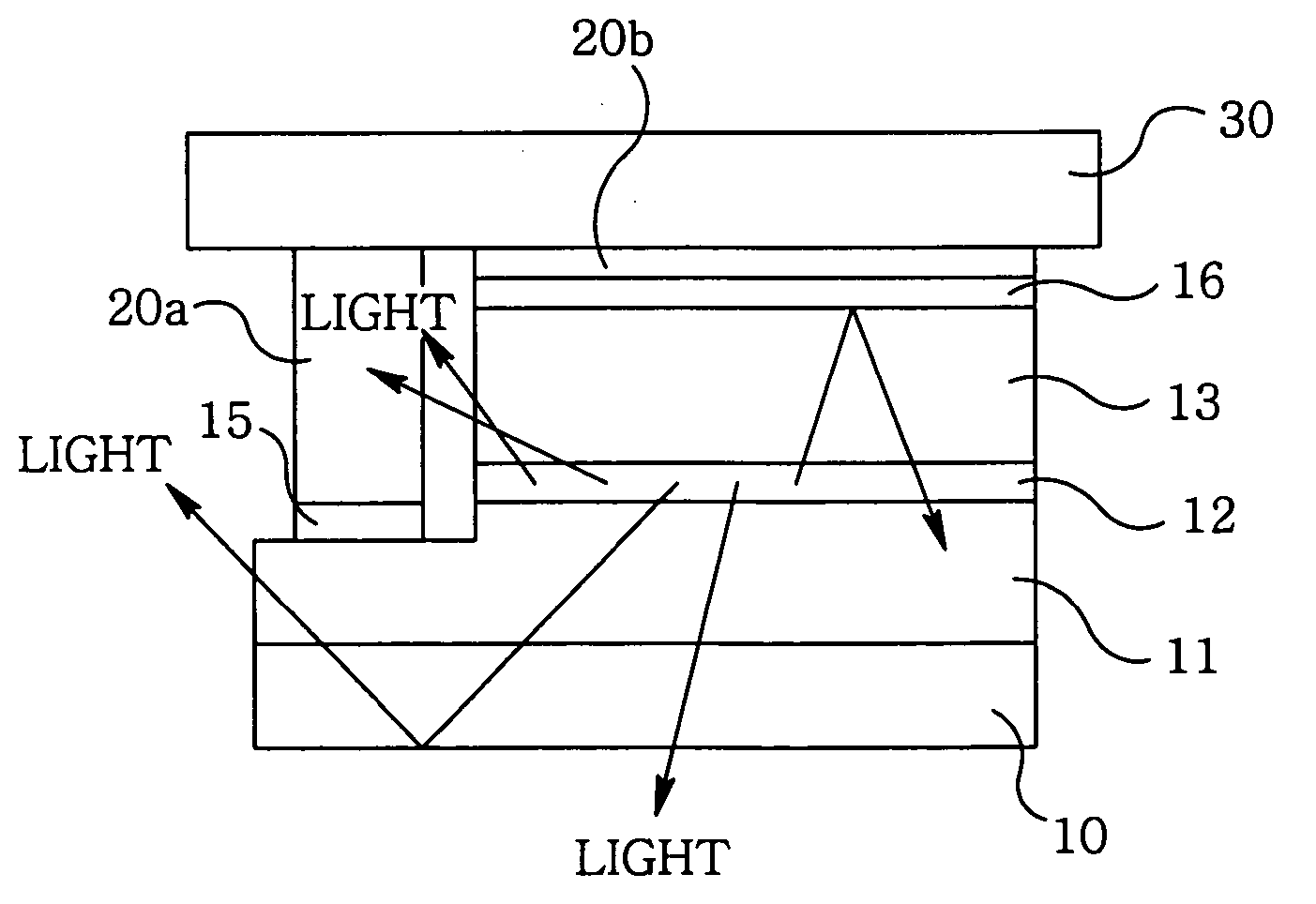
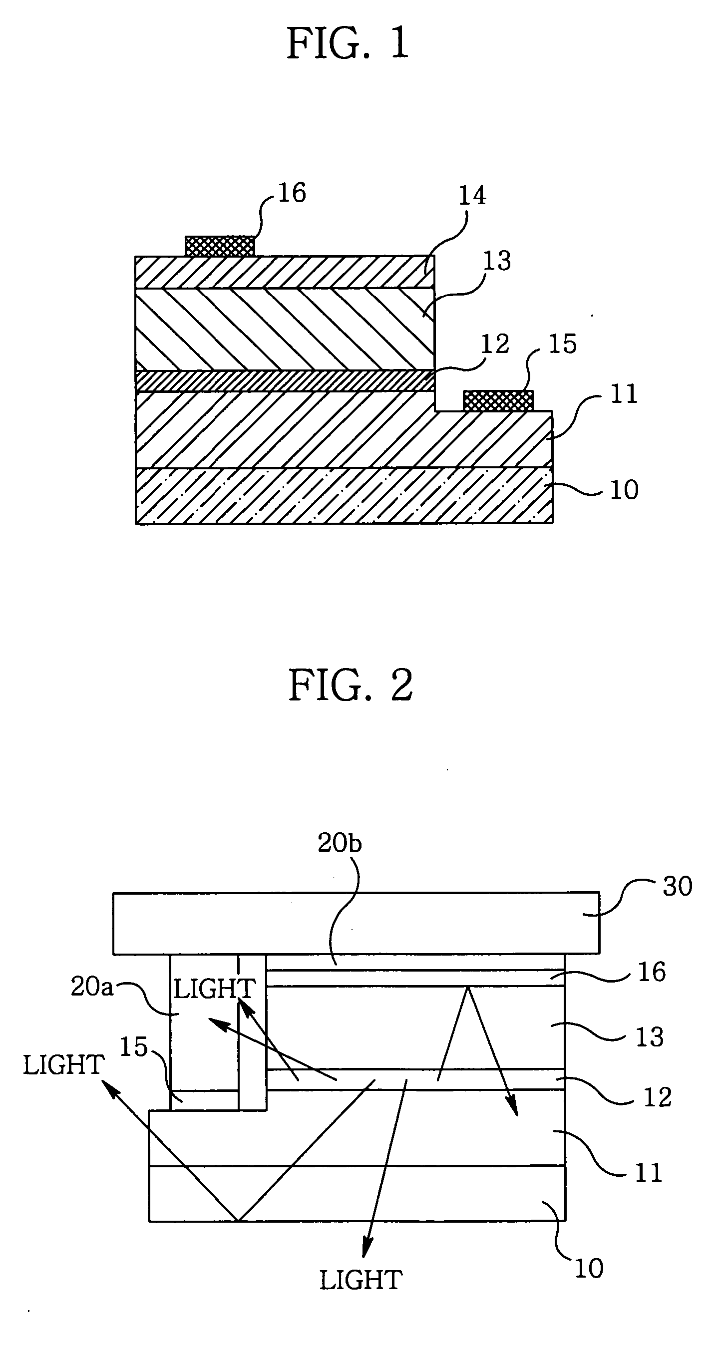
[0034] A substrate (100) is sequentially stacked thereon with an N-type semiconductor layer (110), an active layer (120), and a P-type semiconductor layer (130) (FIG. 3a), and mesa-etching is carried out from the P-type semiconductor layer (130) to portions of the N-type semiconductor layer (110) so that the sidewall thereof is inclined (FIG. 3b).
[0035] In other words, in the process of FIG. 3b, the sidewall is etched at a predetermined angle (α1).
[0036] In order to etch the sidewall having an inclination, a mask layer is formed on the upper surface of the P-type semiconductor (130) except for a region to be etched, and the P-type semiconductor (130) is masked by the mask layer and dry-etched to obtain an inclined sidewall.
[0037] Successively, remaining sidewall of the N-type semiconductor layer (110), the active layer (120) and the P-type semiconduct...
second embodiment
[0047]FIGS. 5a through 5e are cross-sectional views illustrating a fabricating process of a high output LED according to the present invention.
[0048] A substrate (200) is sequentially stacked with an N-type semiconductor layer (210), an active layer (220) and a P-type semiconductor layer (230) (FIG. 5a). Etching is carried out from the P-type semiconductor layer (230) to the N-type semiconductor layer (210) to form an etched sidewall (FIG. 5b). The etched sidewall has a predetermined angle (α3). The substrate (200) is detached from the N-type semiconductor layer (210) (FIG. 5c). Successively, the P-type semiconductor layer (230) is formed thereunder with a reflecting P electrode (240) (FIG. 5d). The inclined sidewall is formed with a reflective film (250) and the N-type semiconductor layer (210) is formed thereon with an N electrode (260) (FIG. 5e). Preferably, a width (W1) of the P-type semiconductor layer (230) is smaller than a width (W2) of the N-type semiconductor layer (210). ...
third embodiment
[0053]FIGS. 7a and 7b are perspective views explaining a fabricating process of a high output LED according to the present invention.
[0054] A substrate (300) is sequentially stacked thereon with a N-type semiconductor layer (310), an active layer (320) and a P-type semiconductor layer (330), and the P-type semiconductor layer (330) is formed thereon with a mask layer (340) formed at a sidewall thereof with indents (341) (FIG. 7a).
[0055] The P-type semiconductor layer (330) is masked by the mask layer (340), and etching is carried out from the P-type semiconductor layer (330) to the N-type semiconductor layer (310). The etched sidewall is formed with inclinations and indents (FIG. 7b).
[0056] Successively, the substrate (300) is detached from the N-type semiconductor layer (310). The reflective P electrode is formed under or underneath the P-type semiconductor layer (330). The inclined sidewall is formed with a reflective film and N electrode is formed on the N-type semiconductor la...
PUM
 Abstract
Description
Claims
Application Information