Stressed field effect transistors on hybrid orientation substrate

a hybrid orientation and transistor technology, applied in the field of stressed field effect transistors on hybrid orientation substrates, can solve the problems of significantly degrading electron mobility on (110) si surfaces, undesirable pfets having larger widths, and completely inappropriate orientation for nfet devices

Inactive Publication Date: 2006-07-06
GLOBALFOUNDRIES INC
View PDF3 Cites 132 Cited by
  • Summary
  • Abstract
  • Description
  • Claims
  • Application Information

AI Technical Summary

Benefits of technology

This patent describes how combining two different techniques can improve the movement of electric current through semiconductors. By creating stress on certain parts of the material, researchers have found that they can increase the speed at which carriers move through it. This results in faster performance for electronic devices made from these materials.

Problems solved by technology

The technical problem addressed in this patent text relates to finding ways to improve the movement of carriers (e.g., electrons and holes) within semiconductor materials like silicon. Current processes and technologies use specific crystal orientations that may favor one type of carrier over another, leading to poor device performance. This patent seeks to provide an improved solution to overcome these limitations and create more efficient semiconductor devices.

Method used


Image

  • Stressed field effect transistors on hybrid orientation substrate
  • Stressed field effect transistors on hybrid orientation substrate
  • Stressed field effect transistors on hybrid orientation substrate

Examples


Embodiment Construction

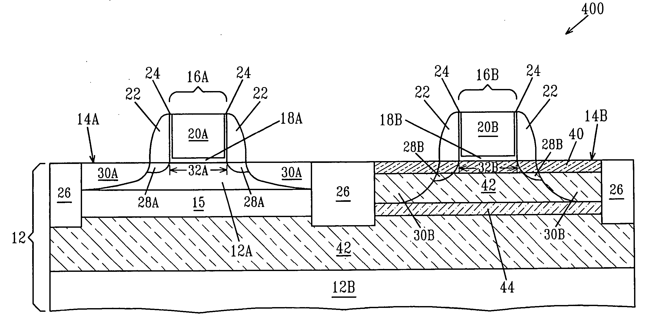
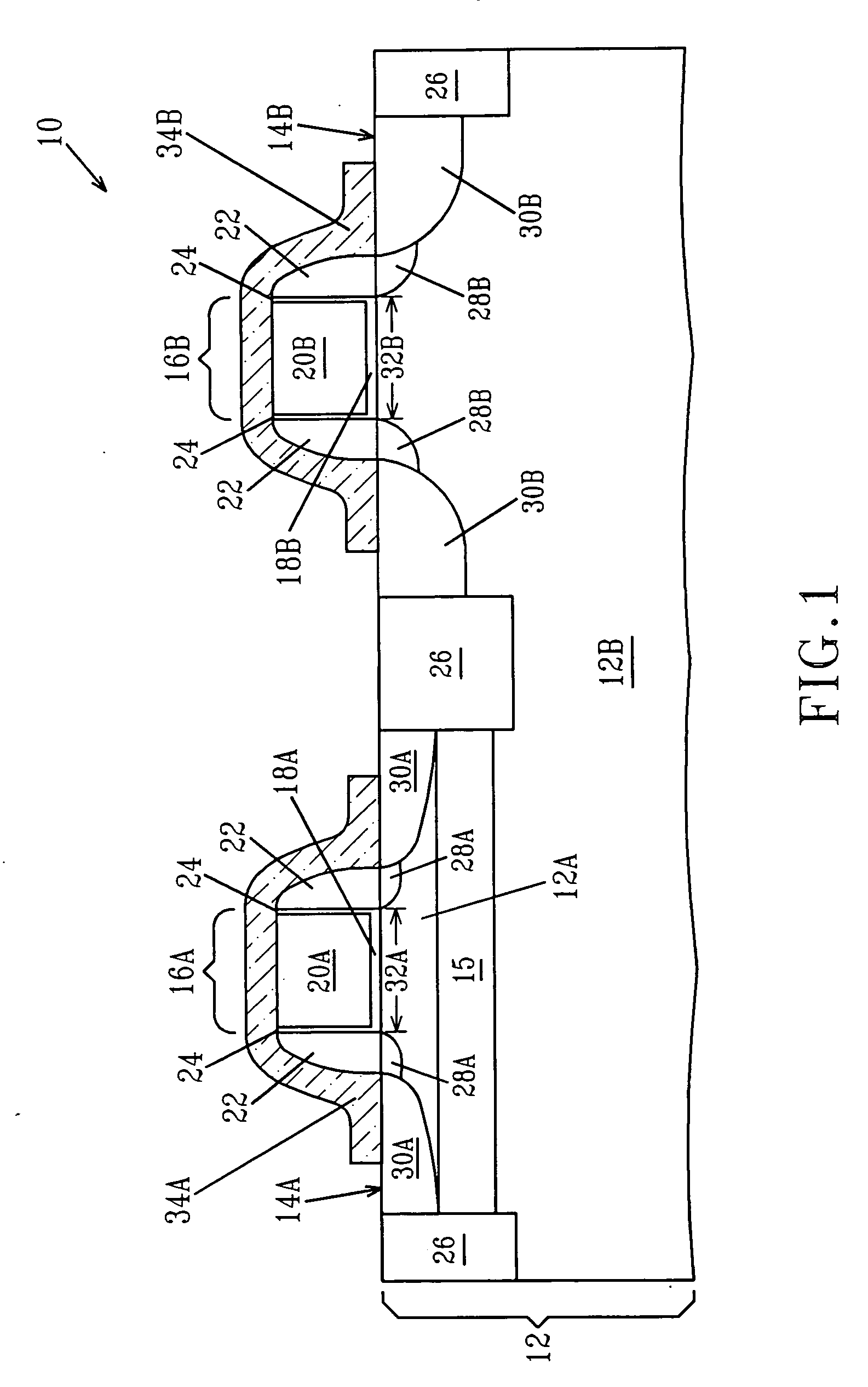
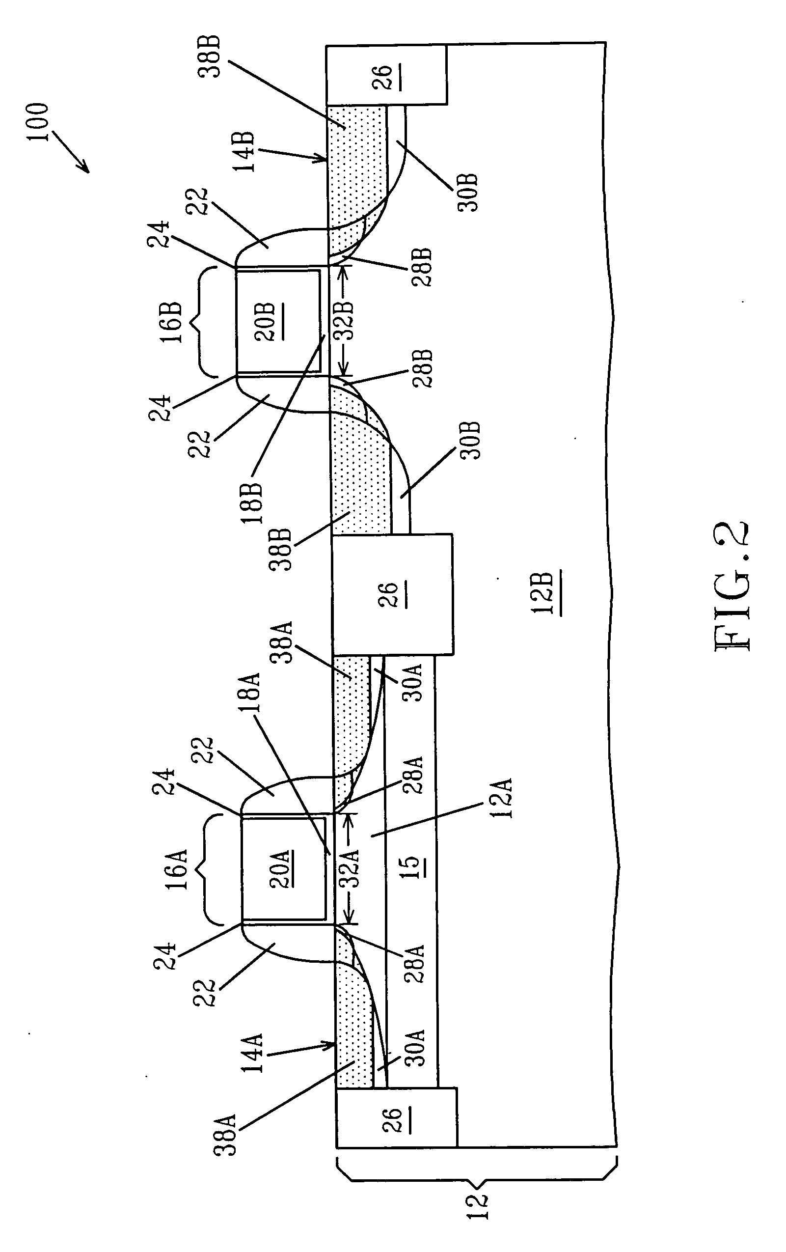
[0024] The present invention, which provides semiconductor structures including stressed channels on a hybrid oriented substrate as well as methods of fabricating the same, will now be described in greater detail by referring to the drawings that accompany the present application. It is noted that the drawings of the present application are provided for illustrative purposes and thus they are not drawn to scale. Moreover, in the drawings, like reference numerals are used in describing like and / or corresponding elements.

[0025] As stated above, the present invention provides semiconductor structures including hybrid orientated substrates having at least two planar surfaces of different crystallographic orientation, and at least one CMOS, e.g., a field effect transistor (FET), located on each planar surface of different crystallographic orientation, wherein each CMOS has a stressed channel. FIGS. 1-7 are pictorial representations of various examples of semiconductor structures that fa...


PUM


Abstract

A semiconductor structure having improved carrier mobility is provided. The semiconductor structures includes a hybrid oriented semiconductor substrate having at least two planar surfaces of different crystallographic orientation, and at least one CMOS device located on each of the planar surfaces of different crystallographic orientation, wherein each CMOS device has a stressed channel. The present invention also provides methods of fabricating the same. In general terms, the inventive method includes providing a hybrid oriented substrate having at least two planar surfaces of different crystallographic orientation, and forming at least one CMOS device on each of the planar surfaces of different crystallographic orientation, wherein each CMOS device has a stressed channel.

Description


Claims


Application Information

Patent Timeline
Owner GLOBALFOUNDRIES INC
Why Eureka
Try Eureka