Coupling methods and architectures for information processing

a technology of information processing and methods, applied in the field of quantum computing, can solve problems such as the identification of methods, the reduction of the decoherence of qubits, and the identification of systems that can support quantum computation

Active Publication Date: 2006-07-06
D WAVE SYSTEMS INC
View PDF6 Cites 184 Cited by
  • Summary
  • Abstract
  • Description
  • Claims
  • Application Information

AI Technical Summary

Benefits of technology

[0047] In some embodiments, the structure further comprises a plurality of flux devices, the plurality of flux devices comprising the first and second flux devices. Such embodiments further comprise a plurality of coupling devices. Each of one or more coupling devices in the plurality of coupling devices comprises a plurality of coupling elements. Furthermore, a first coupling device in the plurality of coupling devices comprises the first and second coupling elements described above. In some embodiments, the structure further comprises a second coupling device comprising third and fourth coupling elements as well as a third flux device comprising first and second lobes. In such embodiments, the third coupling element couples the first lobe of the first flux device with the first lobe of the third flux device and the fourth coupling element couples the second lobe of the first flux device with the first lobe of the third flux device.
[0048] In some embodiments, one or more flux devices in the plurality of flux devices is coupled to two, three, or four flux devices through different coupling devices in the plurality of coupling devices. In some embodiments, a Hamiltonian of a problem to be solved can be mapped onto the plurality of flux devices.
[0049] Another aspect of the present invention provides an apparatus comprising a first and a second information device as well as a coupling device comprising one or more coupling elements. The coupling device is configured to inductively couple the first and second information device devices together. The coupling device is further configured to switch the inductive coupling between ferromagnetic coupling and anti-ferromagnetic coupling of the first and second information devices in a controllable manner. Each coupling element in the coupling device has a dimensionless inductance that is between 0.5 and 2. In some embodiments, the one or more coupling elements consists of two coupling elements that are electrically insulated from each other. In some embodiments, the coupling device further comprises a switch for switching the inductive coupling between ferromagnetic coupling and anti-ferromagnetic coupling of the first and second information devices in a controllable manner. The switch comprises means for concurrently causing: (a) a first coupling element in the one or more coupling elements to go from (i) a first state in which the first coupling element has no coupling strength to (ii) a second state in which the first coupling element has a coupling strength, and (b) a second coupling element in the one or more coupling elements to go from (i) a third state in which the second coupling element has a coupling strength to (ii) a fourth state in which the second coupling element has no coupling strength.
[0050] In some embodiments, the first and second information devices are gradiometric flux devices. In some embodiments, each coupling element in all or a portion of the coupling elements in the one or more coupling elements comprises a dc-SQUID. In some embodiments, each coupling element in all or a portion of the coupling elements in the plurality of coupling elements comprise an rf-SQUID. In some embodiments, the coupling device comprises means for tuning the inductive coupling between the first and second information device on and off. In some embodiments, the coupling device comprises means for tuning a coupling strength of the inductive coupling between the first and second information device.

Problems solved by technology

One limitation in the quantum computing art is the identification of systems that can support quantum computation.
Another limitation in the quantum computing art is the identification of methods that can be used to controllably entangle the states of information devices without introducing a significant source of decoherence.
However, reducing the decoherence of qubits such that many calculations can be performed before information stored in the qubit is destroyed has not been successfully achieved in the art.
Superconducting information devices can be inductively coupled in a direct manner (e.g., without any intervening device), but this type of coupling is typically not controllable, meaning that the strength of the coupling cannot readily be altered.
However, Mooij has the drawback that it is not the ferromagnetic and anti-ferromagnetic coupling types that are switched.
Further, there is no way to completely turn off the coupling in Mooij.
It is possible to turn the INSQUID coupling off, but this is difficult to achieve.
However, the large gain that is needed creates the problem of imprecise balancing of the gradiometric loops of the transformer.
This leads to inaccuracy in maintaining a specified coupling strength.
Also, the transformer is rather large (150 μm×150 μm) and thus infeasible in systems with a large number of devices.
However, such systems are expensive to fabricate and cannot provide full flexibility in adjusting the strength or sign of the coupling.
However, neither reference properly enables the operation of the coupling.

Method used


Image

  • Coupling methods and architectures for information processing
  • Coupling methods and architectures for information processing
  • Coupling methods and architectures for information processing

Examples


example 1

Tunable Coupling of Flux Devices Through an rf-SQUID Transformer

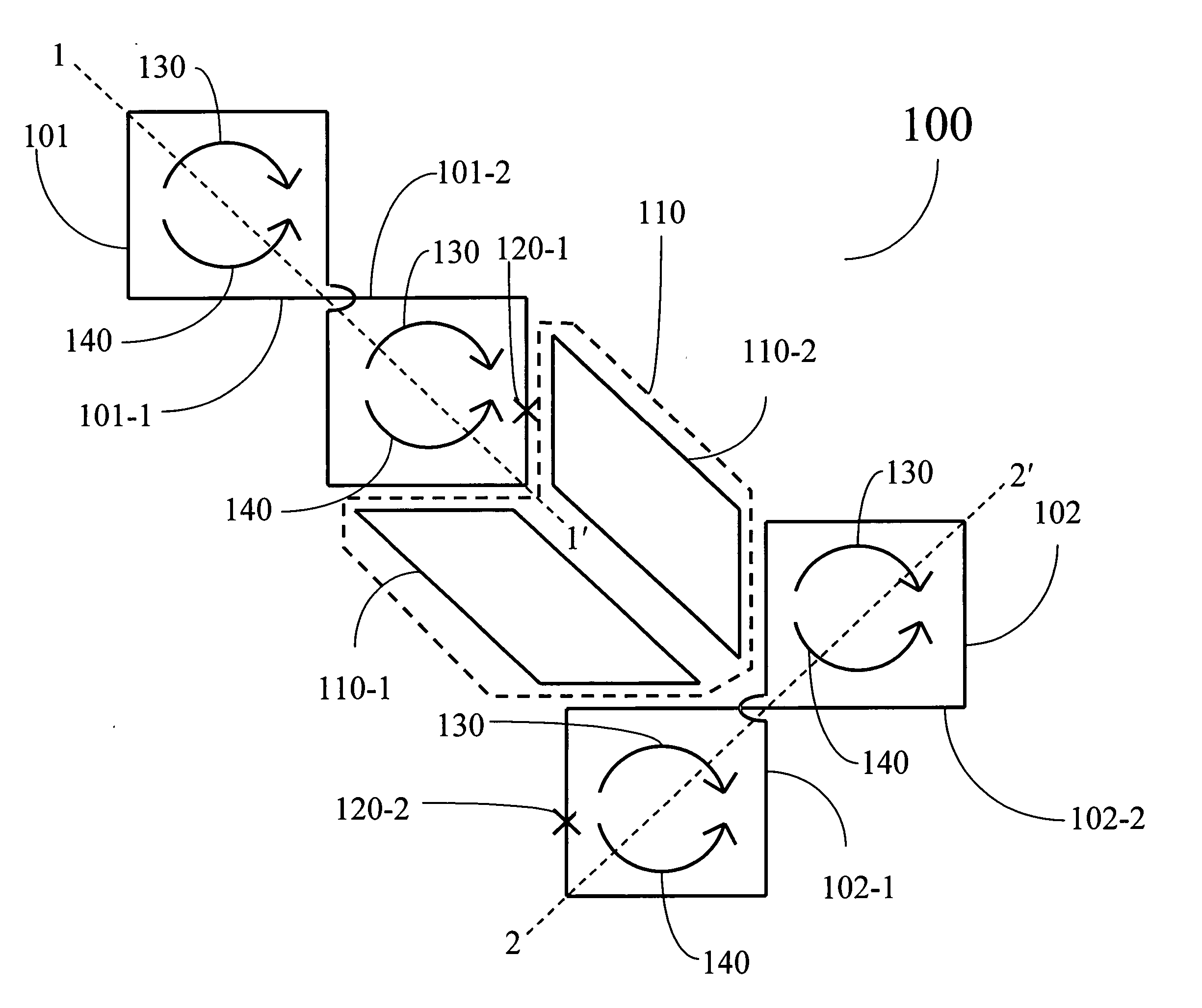
[0119]FIG. 5 illustrates how the dynamics of three rf-SQUIDs 510-a, 510-b, and 510-c, including the tunability of the sign of coupling, can be modeled by an analysis beginning at the classical potential of the rf-SQUIDs. In this example, a, b, c-SQUID or a, b, and c denote rf-SQUIDs 510-a, 510-b, and 510-c, respectively. Hereafter, in this example a, b, and c as a superscript, subscript, or connected to a value or term by a hyphen denotes a value in relation to rf-SQUIDs 510-a, 510-b, and 510-c. Values and quantities drawn to these rf-SQUIDs include but are not limited to:

[0120] L, the rf-SQUID inductance;

[0121] B, the dimensionless SQUID inductance (defined to be equal to 2πLIc / φ0 in SI units, when {overscore (h)}=1 this becomes 4e2LE);

[0122] C, the rf-SQUID capacitance;

[0123] Ic, the critical current of the rf-SQUID; E,the⁢ ⁢rf⁢-⁢SQUID⁢ ⁢Josephson⁢ ⁢energy⁢ ⁢(defined⁢ ⁢to⁢ ⁢be⁢ ⁢h2⁢e⁢Ic);

[0124] Ij, the current o...

example 2

Tunable Coupling of Flux Devices Through a dc-SQUID Transformer

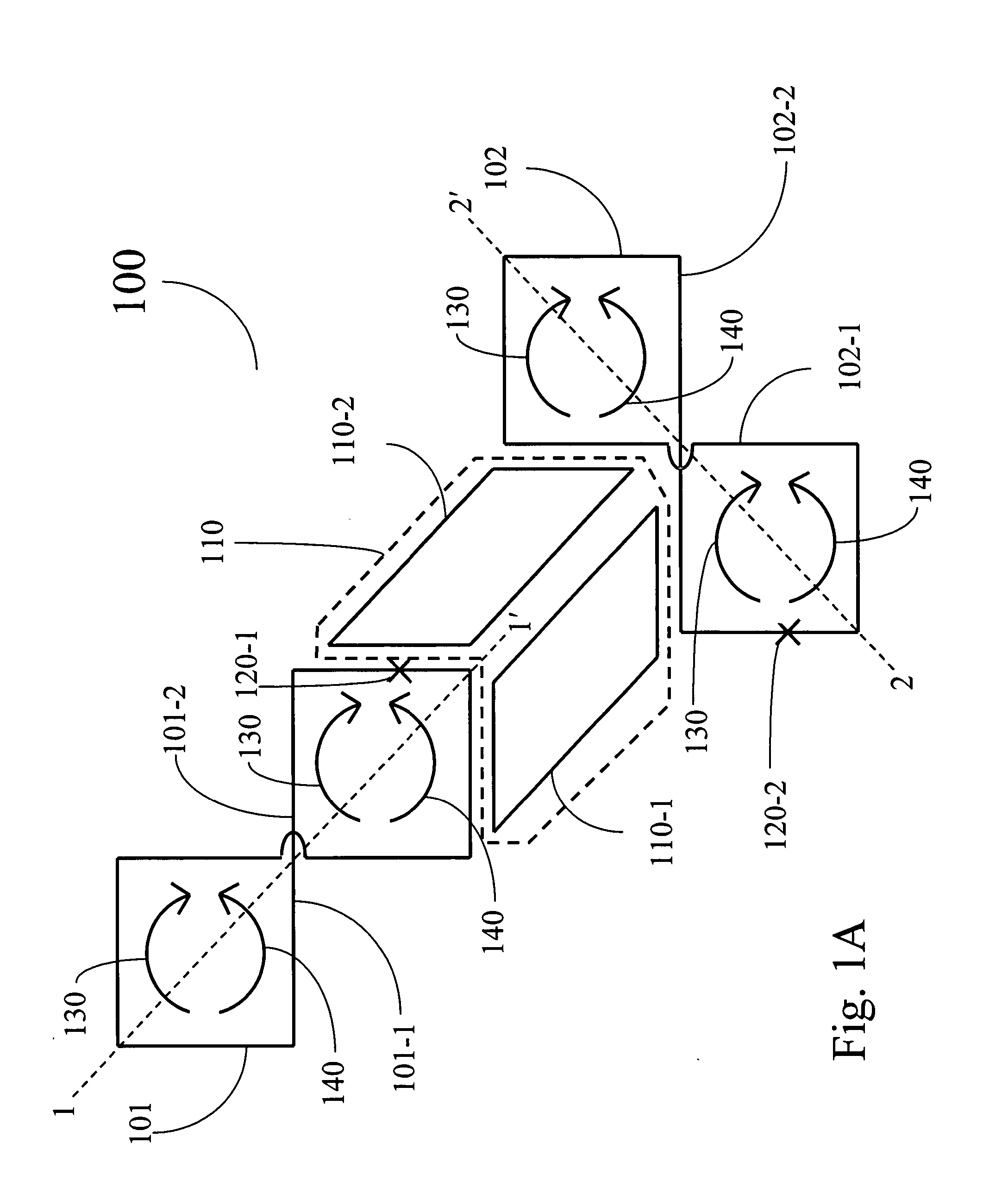
[0142] This example analyzes the set-up depicted in FIG. 7, specifically that of two rf-SQUID flux devices 710-a and 710-c coupled with dc-SQUID 710-b. In the example, a, b, c-SQUID or a, b, and c denote rf-SQUID 710-a, dc-SQUID 710-b, and rf-SQUID 710-c, respectively. Hereafter, in this example a, b, and c as a superscript, subscript, or connected to a value or term by a hyphen denotes a value in relation to SQUIDs 710-a, 710-b, and 710-c. Values and quantities drawn to these SQUIDs include

[0143] L, the SQUID inductance;

[0144]β the dimensionless SQUID inductance (defined to be equal to 2πLIc / Φ0 in SI units; when {overscore (h)}=1 this becomes 4e2LE);

[0145] C, the SQUID capacitance;

[0146] Ic, the SQUID's critical current;

[0147] E, the SQUID Josephson energy (defined⁢ ⁢to⁢ ⁢be⁢ ⁢h2⁢ⅇ⁢Ic);

[0148] Ij, the current of SQUID 710-j, where j=a, b1, b2, or c;

[0149]Φj, the flux of SQUID 510-j, where j=a, b1, b2, or c;

[0150...

example 3

Details and Fabrication of an rf-SQUID

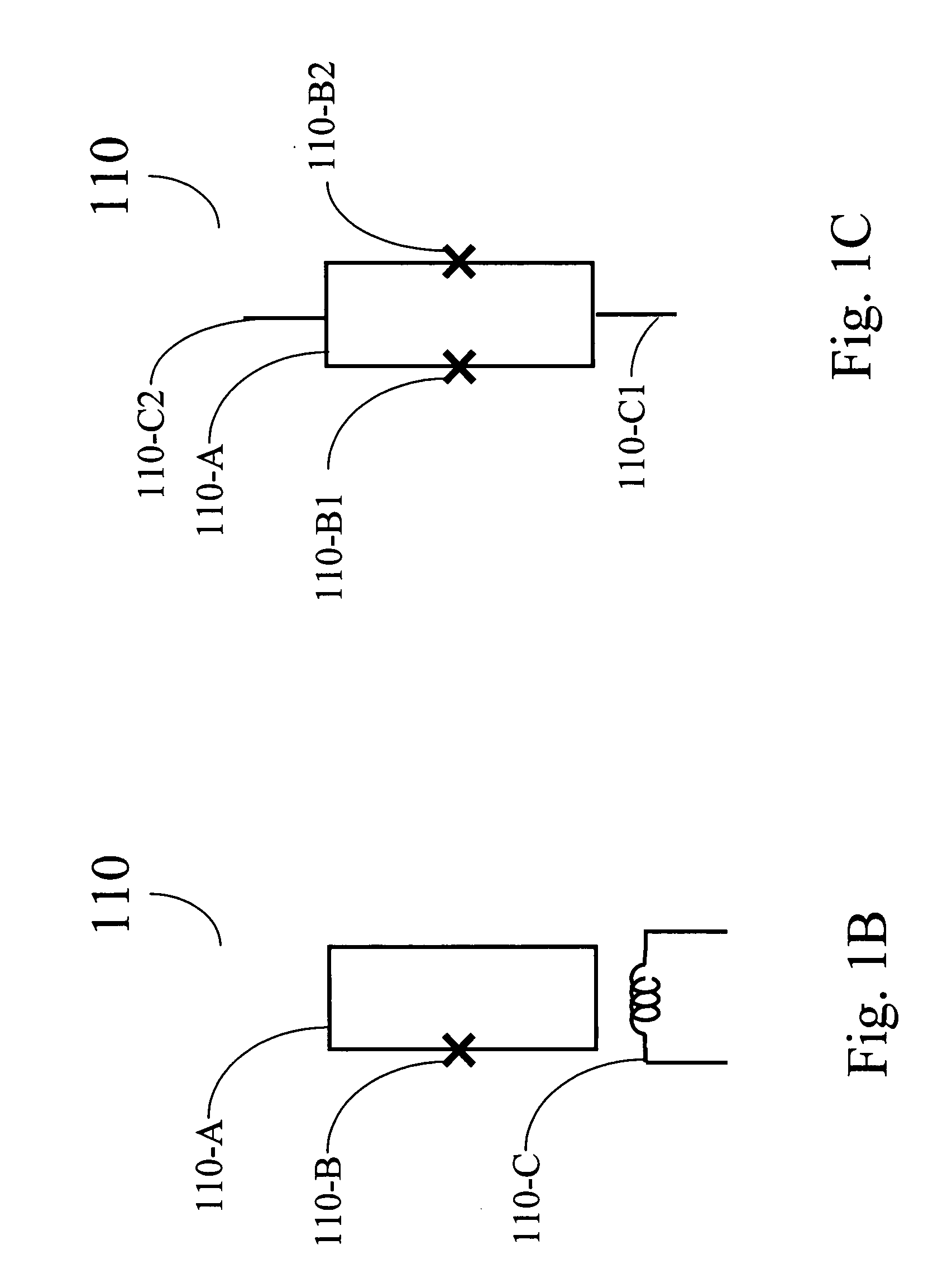
[0160] In some embodiments of the present invention, rf-SQUIDs are used that comprise a superconducting loop that has an inductor and that is interrupted by a single Josephson junction such that the inductor and Josephson junction are in parallel as illustrated in FIG. 11. For a given fabrication process, the Josephson junction is parameterized by its critical current IC, the amount of current it can carry without any dissipation. The rf-SQUID design is then parameterized by the ICL product, where L is the inductance, or its dimensionless inductance 2πLIC / Φ0, where Φ0 is the flux quantum.

[0161] The behavior of the rf-SQUID is described in terms of its response to externally applied flux that is coupled into the SQUID's inductor. For a given applied flux, a circulating current is induced in the SQUID which corresponds to a particular flux state of the SQUID. For values of dimensionless inductance greater than 1, the rf-SQUID can be multi-stable...


PUM


Abstract

A structure comprising (i) a first information device, (ii) a second information device, (iii) a first coupling element and (iv) a second coupling element is provided. The first information device has at least a first lobe and a second lobe that are in electrical communication with each other. The second information device and has at least a first lobe and a second lobe that are in electrical communication with each other. The first coupling element inductively couples the first lobe of the first information device to the first lobe of the second information device. The second coupling element inductively couples the first lobe of the first information device to the second lobe of the second information device.

Description

CROSS REFERENCE TO RELATED APPLICATIONS [0001] This application claims priority to U.S. Patent Application No. 60 / 640,420, filed Dec. 30, 2004, which is hereby incorporated by reference in its entirety.1. FIELD OF THE INVENTION [0002] This invention relates to the field of quantum computing and to the field of superconducting devices. 2. BACKGROUND [0003] In 1982, Richard Feynman proposed that a controllable quantum system could be used to simulate other quantum systems more efficiently than conventional computers. See Feynman, 1982, International Journal of Theoretical Physics 21, pp. 467-488, which is hereby incorporated by reference in its entirety. This controllable quantum system is now commonly referred to as a quantum computer, and effort has been put into developing a general purpose quantum computer that can be used to simulate quantum systems or run specialized quantum algorithms. In particular, solving a model for the behavior of a quantum system commonly involves solving...

Claims


Application Information

Patent Timeline
Patent Type & Authority Applications(United States)
IPC IPC(8): G02B6/34
CPCB82Y10/00G06N99/002G06N10/00G06N99/00H01F37/00H10N60/10
Inventor THOM, MURRAYBERKLEY, ANDREW J.MAASSEN VAN DEN BRINK, ALEXANDER
Owner D WAVE SYSTEMS INC
Why Eureka
Try Eureka