Anisotropic conductive connector and probe member and wafer inspecting device and wafer inspecting method

Inactive Publication Date: 2006-07-06
JSR CORPORATIOON
View PDF6 Cites 14 Cited by
  • Summary
  • Abstract
  • Description
  • Claims
  • Application Information

AI Technical Summary

Benefits of technology

[0056] According to the anisotropically conductive connectors of the present invention, a part to be supported is formed at the peripheral edge of the functional part having the conductive parts for connection in each of the elastic anisotropically conductive films, and this part to be supported is fixed to the periphery about the anisotropically conductive film-arranging hole in the frame plate, so that the anisotropically conductive connectors are hard to be deformed and easy to handle, and the positioning and the holding and fixing to a wafer, which is an object of inspection, can be easily conducted in an electrically connecting operation to the wafer.
[0057] In addition, there is no or little difference in thickness between the conductive parts for connection and the insulating part in the functional part of each of the elastic anisotropically conductive films, so that the mold used in the formation of the elastic anisotropically conductive films has a flat molding surface or a molding surface small in the depth of the recessed parts, and so the movement of the conductive particles is not inhibited when the magnetic field is applied to the molding material layers, and the conductive particles can be easily gathered to portions to become the conductive parts for connection almost without remaining at a portion to become the insulating part in the molding material layer. As a result, good conductivity is surely achieved as to all the conductive parts for connection formed and sufficient insulating property is surely attained between adjoining conductive parts for connection.
[0058] Further, there is no or little difference in height level between the conductive parts for connection and the insulating part in the surface of the functional part of each of the anisotropically conductive films, so that the occurrence of permanent deformation of the conductive parts for connection due to crush of the projected parts thereof is avoided or inhibited even when a wafer, which is an object of inspection, has projected electrodes to be inspected, and so high durability over repeated use is attained.
[0059] According to the cons

Problems solved by technology

The anisotropically conductive elastomer sheet is flexible and easy to be deformed, and so it is low in handling property.
Therefore, the positioning and the holding and fixing of the uneven distribution type anisotropically conductive elastomer sheet are becoming to be difficult upon its electrical connection to electrodes to be inspected of the object of inspection.
In the burn-in test, there is a problem that even when the necessary positioning, and holding and fixing of the uneven distribution type anisotropically conductive elastomer sheet to an integrated circuit device has been realized once, positional deviation between conductive parts of the uneven distribution type anisotropically conductive elastomer sheet and electrodes to be inspected of the integrated circuit device occurs when they are subjected to thermal hysteresis by temperature change, since a coefficient of thermal expansion is greatly different between a material (for example, silicon) making up the integrated circuit device that is the object of inspection, and a material (for example, silicone rubber) making up the uneven distribution type anisotropically conductive elastomer sheet, as a result, the electrically connected state is changed, and thus the stably connected state is not retained.
According to such an anisotropically conductive connector, it is hard to be deformed and easy to handle because the anisotropically conductive elastomer sheet is supported by the metal-made frame plate.
In a burn-in test on the other hand, it takes a long time to individually conduct electrical inspection of a great number of integrated circuit devices because each integrated circuit device that is an object of inspection is fine, and its handling is inconvenient, whereby inspection cost becomes considerably high.
When a wafer that is an object of inspection is of large size of, for example, at least 8 inches in diameter, and the number of electrodes to be inspected formed thereon is, for example, at least 5,000, particularly at least 10,000, however, the following problems are involved when the above-described anisotropically conductive connector is applied as a probe member for the probe test or WLBI test, since a pitch between electrodes to be inspected in each integrated circuit is extremely small.
However, such an anisotropically conductive elastomer sheet is large in the whole area, but each conductive part is fine, and the area proportion of the surfaces of the conductive parts to the whole su

Method used


Image

  • Anisotropic conductive connector and probe member and wafer inspecting device and wafer inspecting method
  • Anisotropic conductive connector and probe member and wafer inspecting device and wafer inspecting method
  • Anisotropic conductive connector and probe member and wafer inspecting device and wafer inspecting method

Examples


Example

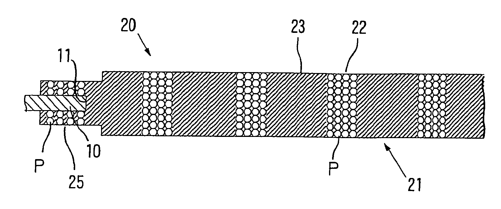
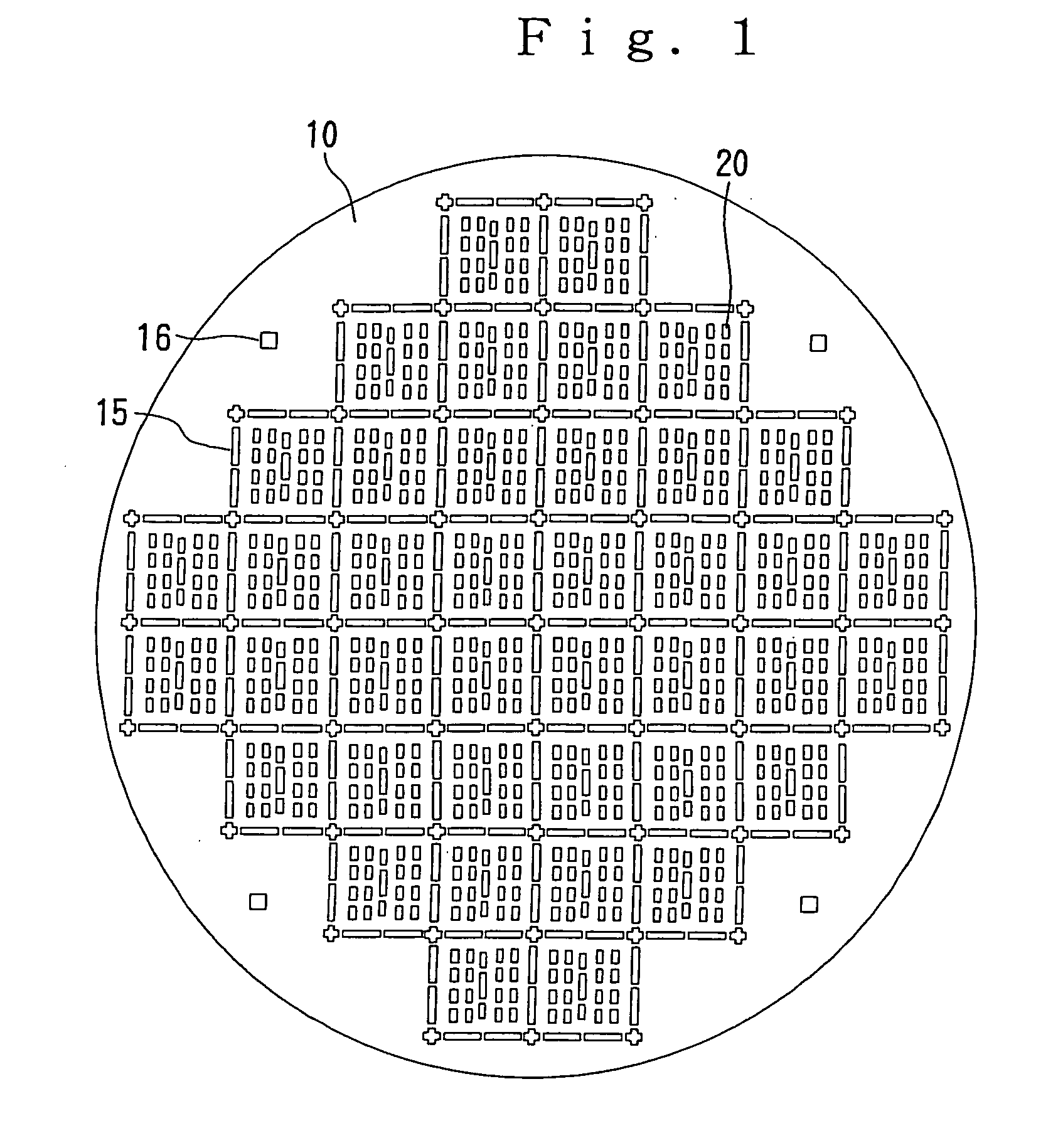
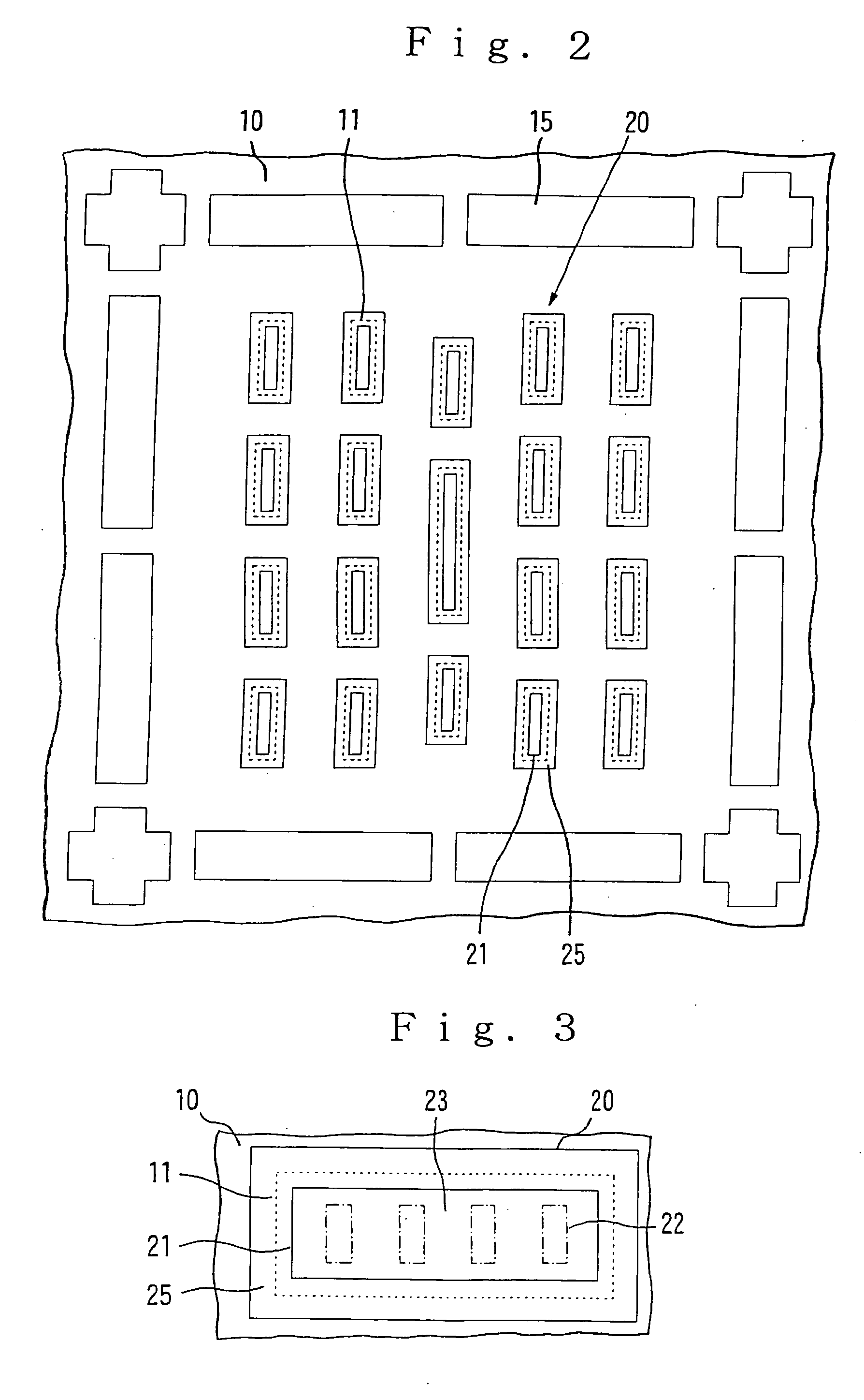
[0094]1 Probe member, [0095]2 Anisotropically conductive connector, [0096]3 Pressurizing plate, [0097]4 Wafer mounting table, [0098]5 Heater, [0099]6 Wafer, [0100]7 Electrodes to be inspected, [0101]10 Frame plate, [0102]11 Anisotropically conductive film-arranging holes, [0103]15 Air circulating holes, [0104]16 Positioning holes, [0105]20 Elastic anisotropically conductive films, [0106]20A Molding material layers, [0107]21 Functional parts, [0108]22 Conductive parts for connection, [0109]23 Insulating part, [0110]24 Projected parts, [0111]25 Parts to be supported, [0112]26 Conductive parts for non-connection, [0113]30 Circuit board for inspection, [0114]31 Inspection electrodes, [0115]40 Sheet-like connector, [0116]41 Insulating sheet, [0117]42 Electrode structures, [0118]43 Front-surface electrode parts, [0119]44 Back-surface electrode parts, [0120]45 Short circuit parts, [0121]50 Chamber, [0122]51 Evacuation pipe, [0123]55 O-rings, [0124]60 Mold, [0125]61 Top force, [0126]62 Base...


PUM


Abstract

An anisotropically conductive connector including elastic anisotropically conductive films each having a functional part, in which a plurality of conductive parts for connection containing conductive particles and extending in a thickness-wise direction of the film have been arranged in a state mutually insulated by an insulating part. Assuming that a thickness of the conductive parts for connection in the functional part of the elastic anisotropically conductive film is T1 and a thickness of the insulating part in the functional part is T2, a ratio (T2/T1) is at least 0.9

Description

TECHNICAL FIELD [0001] The present invention relates to an anisotropically conductive connector suitable for use in conducting electrical inspection of a plurality of integrated circuits formed on a wafer in a state of the wafer, a probe member equipped with this anisotropically conductive connector, a wafer inspection apparatus equipped with this probe member, and a wafer inspection method using this probe member, and particularly to an anisotropically conductive connector suitable for use in conducting electrical inspection of integrated circuits, which are formed on a wafer having a diameter of, for example, 8 inches or greater and have at least 5,000 electrodes to be inspected in total, in a state of the wafer, a probe member equipped with this anisotropically conductive connector, a wafer inspection apparatus equipped with this probe member, and a wafer inspection method using this probe member. BACKGROUND ART [0002] In the production process of semiconductor integrated circuit...

Claims


Application Information

Patent Timeline
IPC IPC(8): H01R4/58G01R1/073G01R31/28H01R11/01
CPCG01R1/0735G01R1/07378G01R31/2889H01R11/01H01L22/00G01R1/06
Inventor NAOI, MASAYA
Owner JSR CORPORATIOON
Why Eureka
Try Eureka