Semiconductor device and computer program product for designing the same

a technology of semiconductor devices and computer programs, applied in semiconductor devices, semiconductor/solid-state device details, electrical apparatus, etc., can solve problems such as deteriorating wiring performance, and achieve the effects of reducing the amount of layout data, reducing the computing load in processing layout data, and improving wiring performan

Inactive Publication Date: 2006-07-13
NEC ELECTRONICS CORP
View PDF0 Cites 207 Cited by
  • Summary
  • Abstract
  • Description
  • Claims
  • Application Information

AI Technical Summary

Benefits of technology

[0010] According to the present invention, as described above, the plurality of vias are arranged only at the above-mentioned partial intersections. It is therefore possible to route wires freely in a region where the vias are not placed. Therefore, the wiring performance is improved. Moreover, since the plurality of vias are arranged only at the partial intersections, it is possible to reduce the amount of layout data that is produced at the time of the computer-aided designing. Therefore, computing load in processing the layout data is reduced.
[0011] Furthermore, according to the present invention, the plurality of vias are arranged regularly (systematically) in accordance with a predetermined rule. As a result, data (language) describing the vias in the above-mentioned layout data also have certain regularity. Thus, data compression rate with respect to the layout data is improved. Therefore, computing load in processing the layout data is reduced.
[0012] The above-mentioned structure of the power supply wires can be applied to an ASIC (Application Specific Integrated Circuit). In this case, the structure of the power supply wires acc

Problems solved by technology

This deteriorates

Method used


Image

  • Semiconductor device and computer program product for designing the same
  • Semiconductor device and computer program product for designing the same
  • Semiconductor device and computer program product for designing the same

Examples


Embodiment Construction

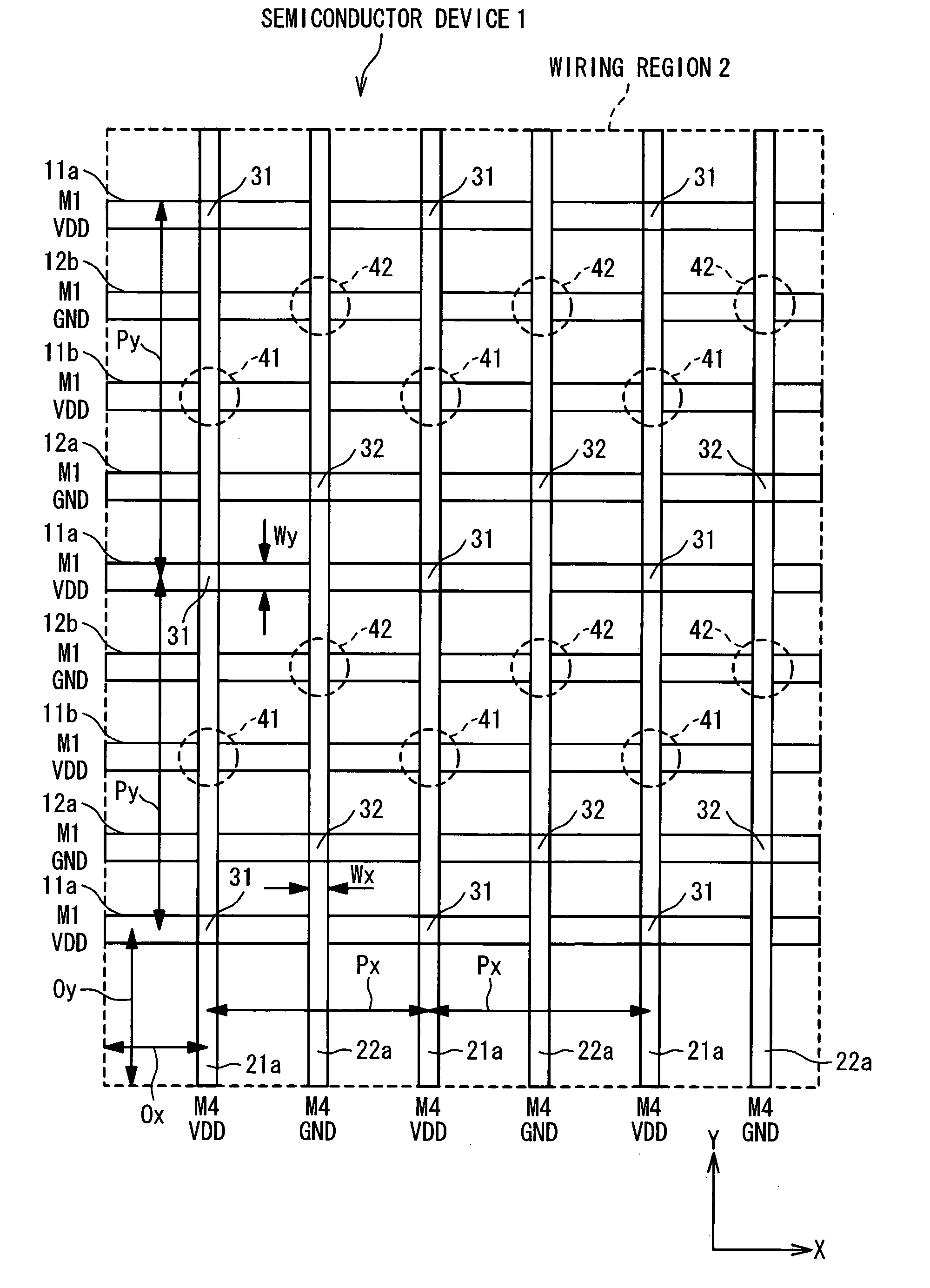
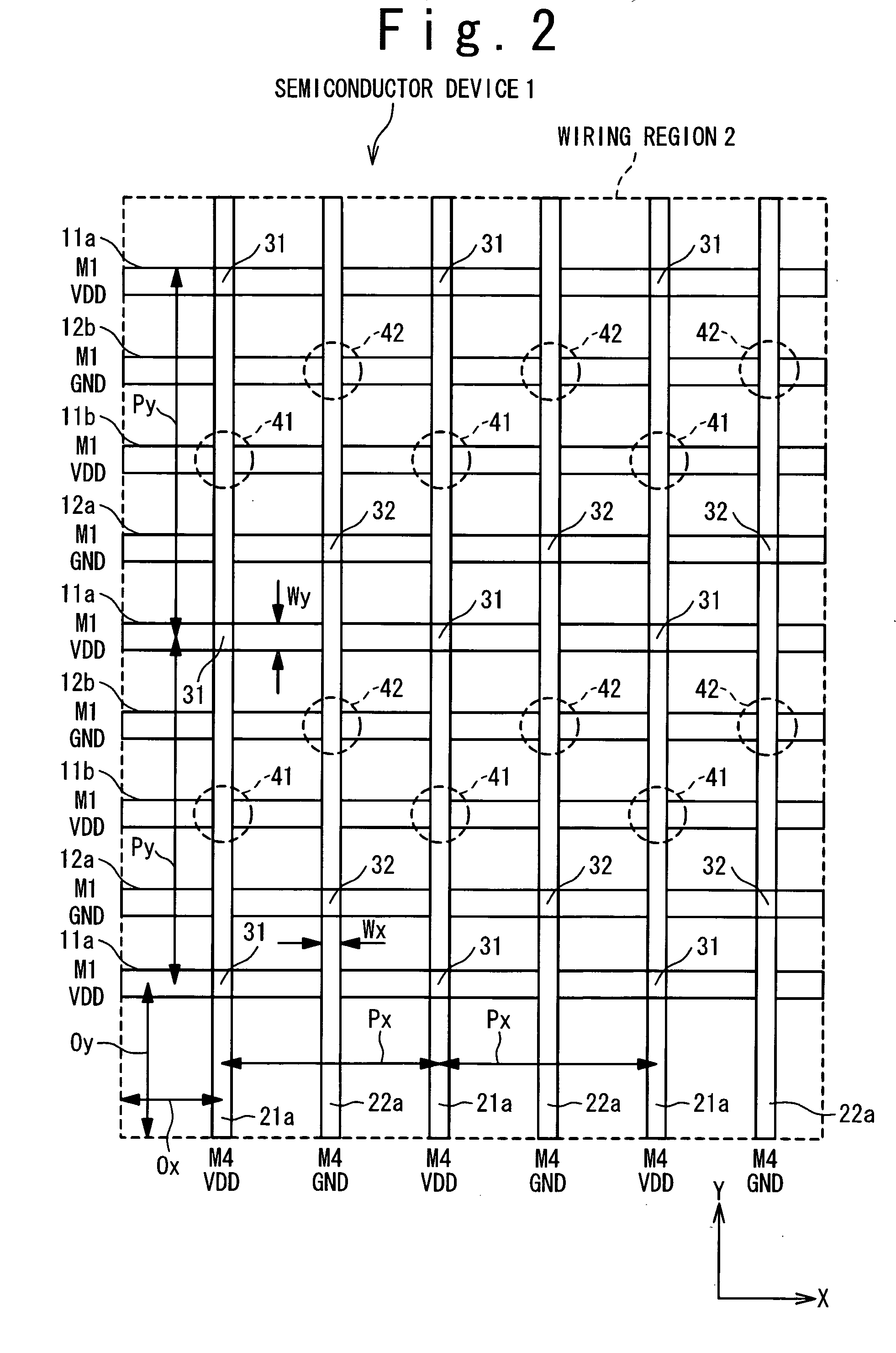
[0024] The invention will be now described herein with reference to illustrative embodiments. Those skilled in the art will recognize that many alternative embodiments can be accomplished using the teachings of the present invention and that the invention is not limited to the embodiments illustrated for explanatory purposed. A semiconductor device, a semiconductor device design system and a semiconductor device design program will be described below with reference to the accompanying drawings.

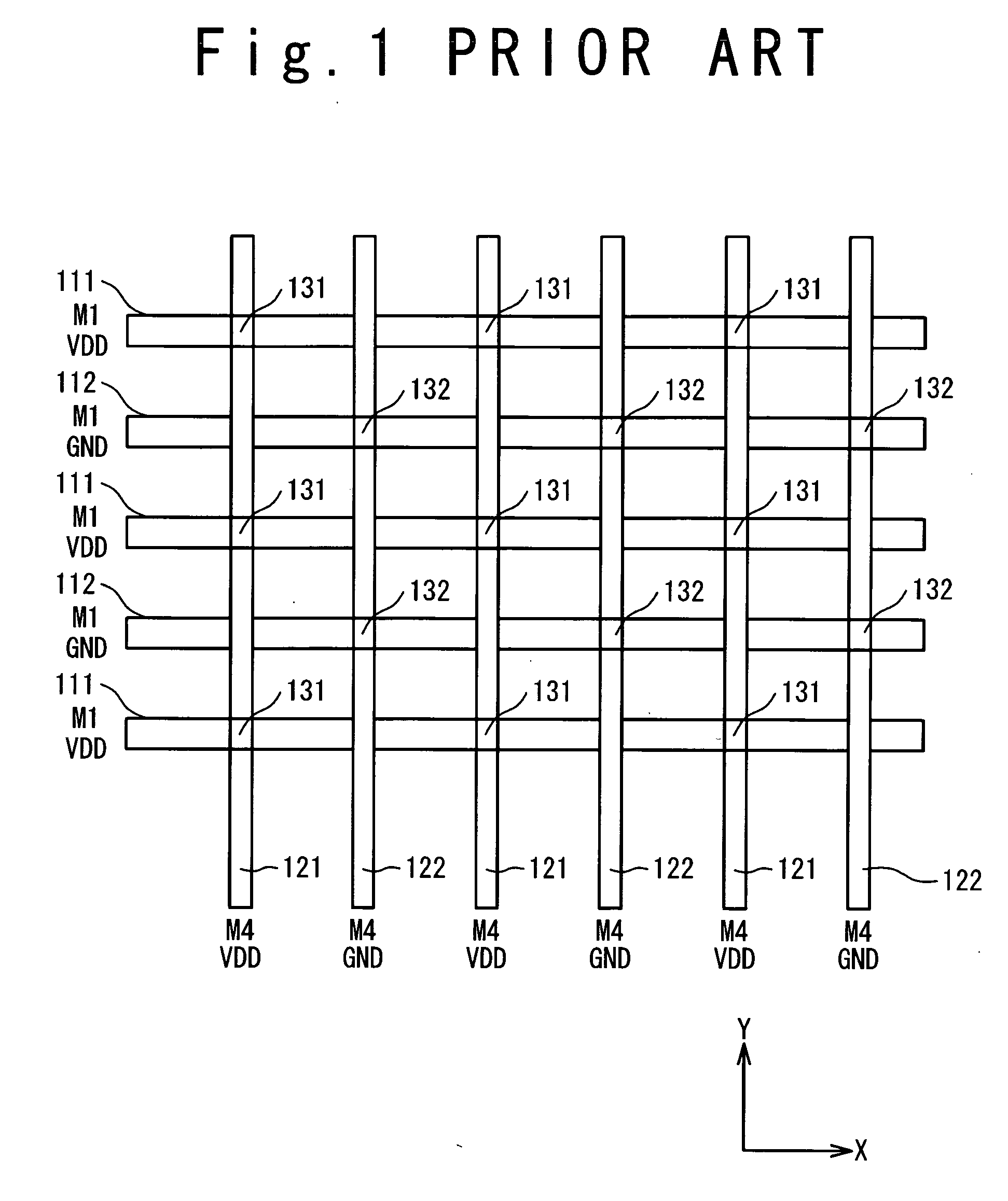
[0025]FIG. 2 is a plan view showing a structure of a semiconductor device 1 according to the embodiment of the present invention. The plane in the figure is defined by X and Y directions that are orthogonal to each other. An arrangement of power supply wires (including power supply lines and ground lines) in a wiring region 2 is schematically shown in FIG. 2.

[0026] The semiconductor device 1 has multiple wiring layers. In a wiring layer M1 of the multiple wiring layers, for example, a plural...


PUM


Abstract

A semiconductor device has: a plurality of first power supply wires formed in a first wiring layer; a plurality of second power supply wires formed in a second wiring layer; and a plurality of vias connecting between the first wiring layer and the second wiring layer. The plurality of second power supply wires overlap the plurality of first power supply wires at a plurality of intersections. The plurality of vias are arranged regularly at a part of the plurality of intersections.

Description

BACKGROUND OF THE INVENTION [0001] 1. Field of the Invention [0002] The present invention relates to a semiconductor device and a technology for designing the semiconductor device. In particular, the present invention relates to a layout of power supply wires in a semiconductor device. [0003] 2. Description of the Related Art [0004] In designing an LSI, it is essential to utilize a computer in order to reduce time for the designing and verifying and eliminate human errors. Such a system utilizing a computer for designing a semiconductor device is called a CAD (Computer Aided Design) system. According to a cell-based LSI design method, a plurality of cells are developed as a library. A designer designs an LSI by using the CAD and arranging desired cells in a layout space defined on the computer. As a result, a layout data representing a configuration of the designed LSI can be generated. [0005] In a conventional LSI designing, power supply wires (power supply lines, ground lines) are...

Claims


Application Information

Patent Timeline
IPC IPC(8): H01L27/10
CPCH01L27/10
Inventor OHSHIGE, SHINICHIRO
Owner NEC ELECTRONICS CORP
Why Eureka
Try Eureka