Memory technology test apparatus

a memory technology and test apparatus technology, applied in the field of memory devices, can solve the problems of spurious data to be used during read or write operations, adversely affecting data and address eyes, and other high-speed memory devices currently being developed, and achieve the effects of quick, flexible, efficient and inexpensive manner, inexpensive and timely, and cheap and convenient us

Inactive Publication Date: 2006-07-13
JEDDELOH JOSEPH M
View PDF3 Cites 1 Cited by
  • Summary
  • Abstract
  • Description
  • Claims
  • Application Information

AI Technical Summary

Benefits of technology

[0007] The present invention provides a mechanism for testing and evaluating memory technology in a quick, flexible, efficient and inexpensive manner.
[0008] The above and other features and advantages are achieved by a programmable control device that creates an environment for controlling, testing and evaluating memory designs. The control device provides automated testing of address eyes, data eyes and voltage margins. The control device interfaces with a conventional computer system, such as a personal computer (PC). The computer system gathers test data and outputs the data in a graphical format if desired. Since the control device is quickly re-programmable, new memory sequencing, control, timing and power techniques are rapidly proto-typed in an inexpensive and timely manner.

Problems solved by technology

Designing a DDR SDRAM and an interface for the DDR SDRAM, as well as other high speed memory devices currently being developed, is a complex, time consuming and expensive process.
Clock skews may adversely effect data and address eyes (i.e., the short period of time in which the data and address information is reliable / valid).
This may cause spurious data to be used during read or write operations.
In addition, voltage margins may adversely effect the operation of the DDR SDRAM and its power consumption.
This process is expensive and time consuming.
As can be appreciated, the development of new memory devices takes a substantial amount of time, is expensive, wasteful and inefficient.

Method used


Image

  • Memory technology test apparatus
  • Memory technology test apparatus
  • Memory technology test apparatus

Examples


Embodiment Construction

[0016] In the following detailed description, reference is made to various specific embodiments in which the invention may be practiced. These embodiments are described with sufficient detail to enable those skilled in the art to practice the invention, and it is to be understood that other embodiments may be employed, and that structural and electrical changes may be made without departing from the spirit or scope of the present invention.

[0017] The following description is made with reference to DDR SDRAM technology. It should be appreciated, however, that the test board and control device of the present invention may be utilized with any current and future memory technology and that the invention is not to be limited to any specific form of memory (such as a DDR SDRAM). In fact, one of the objectives of the invention is to aid in the development of new technology by simplifying the testing, evaluation and prototyping of new memory devices.

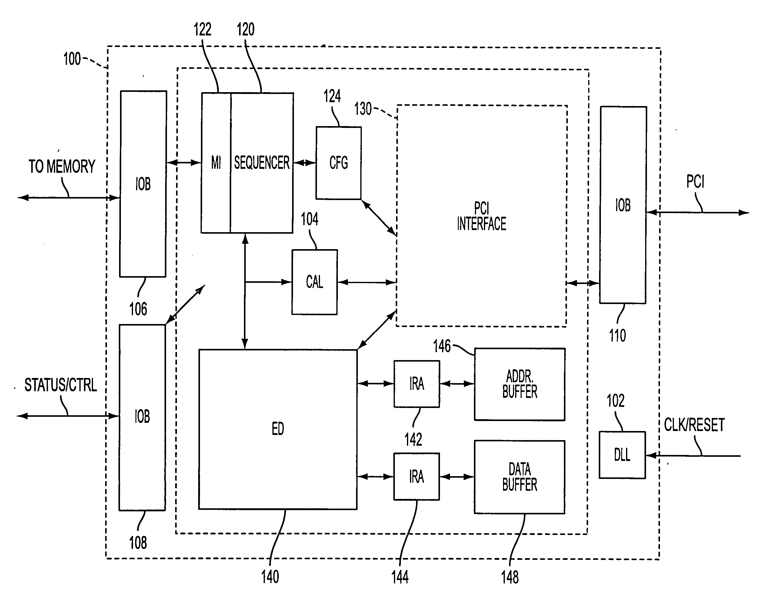
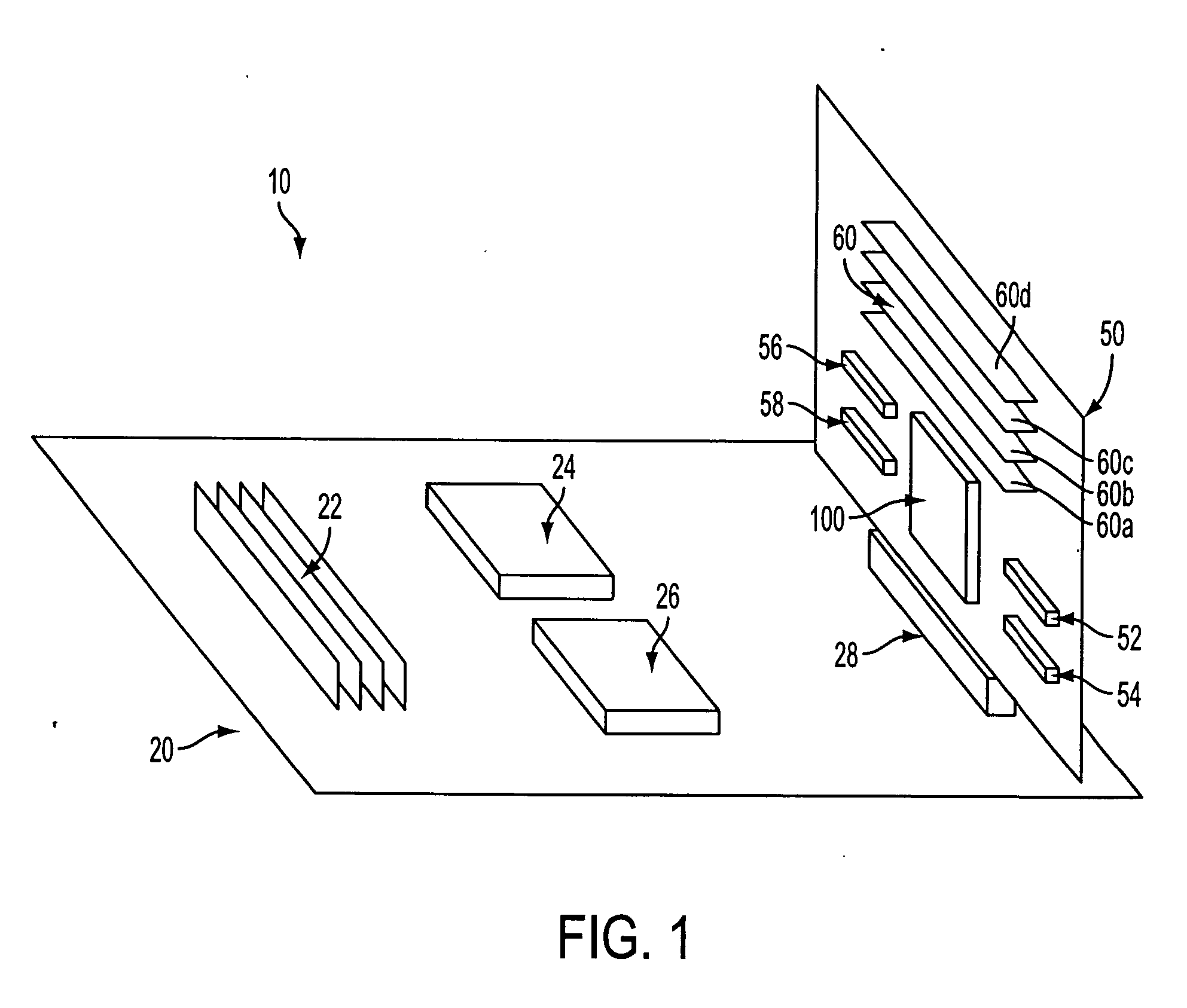
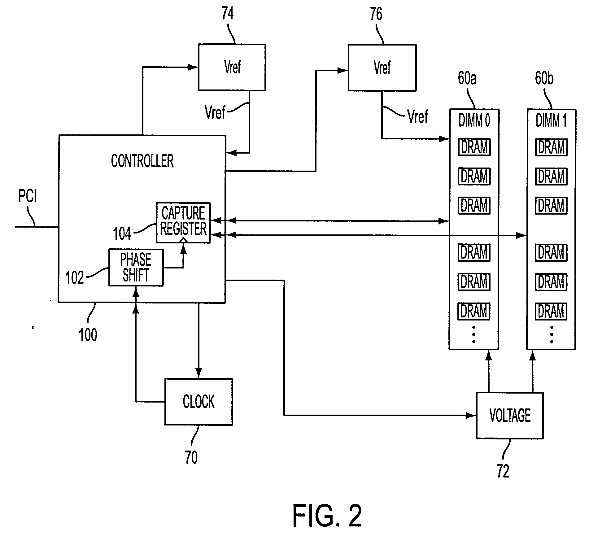
[0018]FIG. 1 illustrates an exemplary t...


PUM


Abstract

A programmable control device that creates an environment for controlling, testing and evaluating memory designs. The control device provides automated testing of address eyes, data eyes and voltage margins. The control device interfaces with a conventional computer system, such as a personal computer (PC). The computer system gathers test data and outputs the data in a graphical format if desired. Since the control device is quickly re-programmable, new memory sequencing, control, timing and power techniques are rapidly proto-typed in an inexpensive and timely manner.

Description

FIELD OF THE INVENTION [0001] The present invention relates generally to memory devices and, more particularly to a mechanism for testing and evaluating current and new memory technologies. BACKGROUND OF THE INVENTION [0002] As processor speeds continue to increase, memory system designers are under increasing pressure to create memory devices that can input and output data at increasingly faster rates. As such, new memory system designs are constantly being proposed, tested and, if satisfactory, manufactured. [0003] Double data rate (DDR) synchronous dynamic random access memory (SDRAM) devices are a relatively new form of memory device that was designed to help bridge the gap between processor and memory speeds. During read operations, DDR SDRAM devices return a data clock signal (or data strobe) along with the data, and this data clock signal is used to clock the data into the processor (or into a memory controller attached to the processor). The strobe is typically supplied at t...

Claims


Application Information

Patent Timeline
Patent Type & Authority Applications(United States)
IPC IPC(8): G11C29/00G11C29/56
CPCG11C29/56G11C2029/5004
Inventor JEDDELOH, JOSEPH M.
Owner JEDDELOH JOSEPH M
Why Eureka
Try Eureka