Heat sink for surface-mounted semiconductor devices

a technology for semiconductor devices and heat sinks, which is applied in semiconductor devices, semiconductor/solid-state device details, cooling/ventilation/heating modifications, etc., can solve the problems of increasing manufacturing costs, increasing costs, and inadmissible heating of adjacent semiconductor devices

Inactive Publication Date: 2006-07-20
INFINEON TECH AG
View PDF12 Cites 46 Cited by
  • Summary
  • Abstract
  • Description
  • Claims
  • Application Information

AI Technical Summary

Problems solved by technology

One disadvantage to this design is impermissible heating of adjacent semiconductor devices.
A further disadvantage is the high material outlay, which thus increases the costs.
Yet another disadvantage is that, in addition to producing the covers, it is also necessary to produce clamping elements in the form of clips, which increases the manufacturing costs.
In this design, there is the risk of impermissible heating of adjacent semiconductor devices which intrinsically generate a reduced power loss and are then impermissibly additionally heated by the heat distribution of the thermally conductive substance and the thermally conductive covers.
Moreover, there is also the disadvantage of an increased material outlay, which increases manufacturing costs.
Solutions of this type have the disadvantage that, in mechanical shock tests and in vibration tests and also in the case of other manual influences, an impermissibly high mechanical stress may be exerted on the devices to be cooled by virtue of the heat sink bonded on adhesively, which may result in damage to the semiconductor device.

Method used


Image

  • Heat sink for surface-mounted semiconductor devices
  • Heat sink for surface-mounted semiconductor devices
  • Heat sink for surface-mounted semiconductor devices

Examples


Embodiment Construction

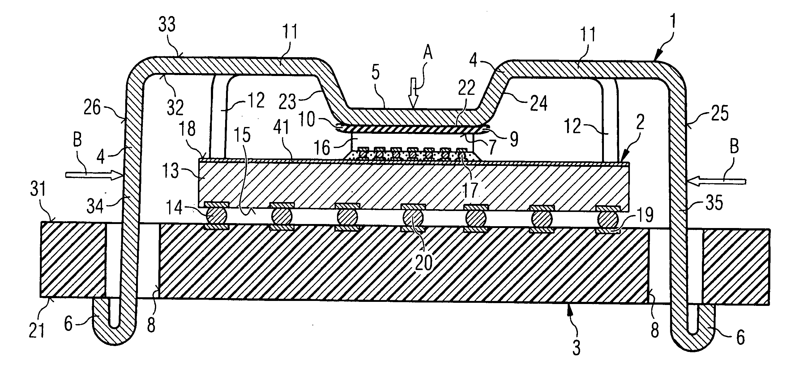
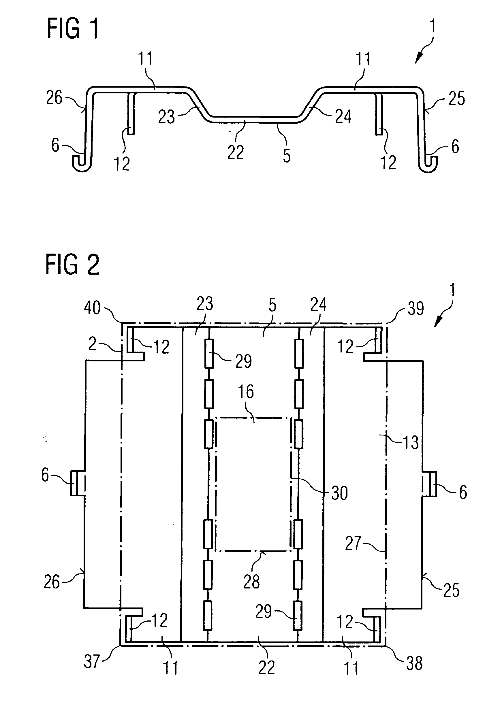
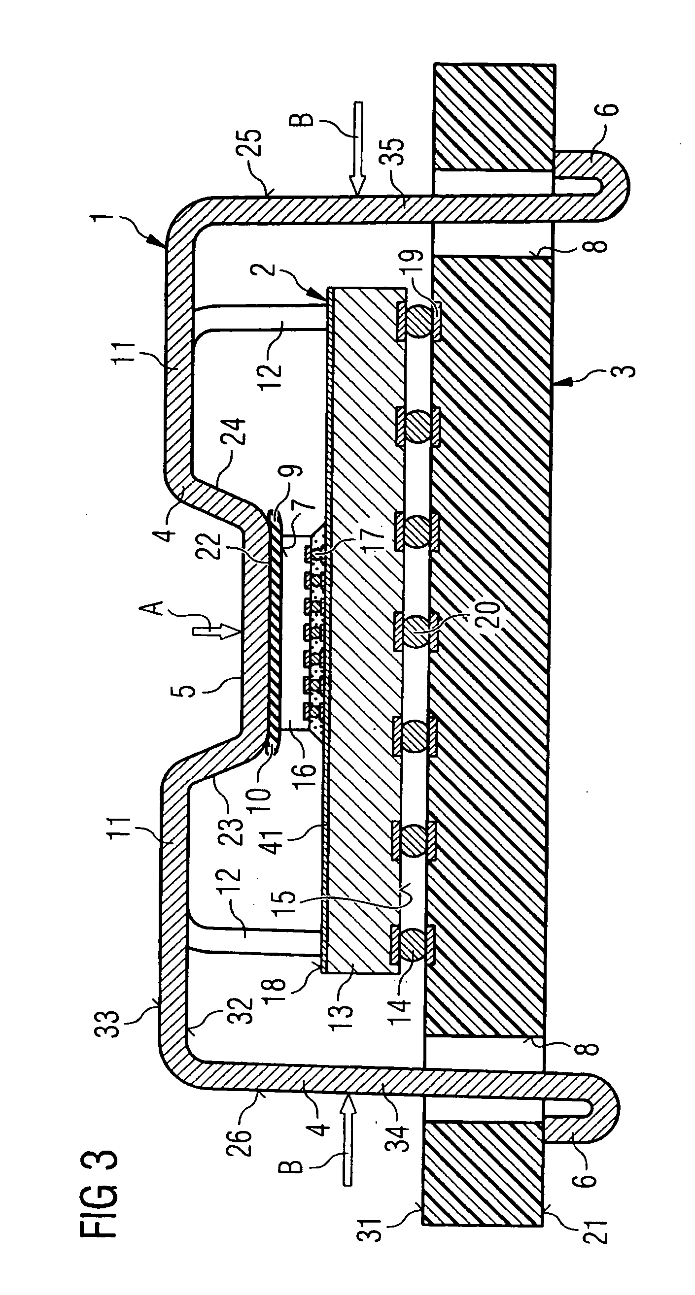
[0026] In accordance with the invention, a heat sink is provided for surface-mounted semiconductor devices on a main circuit board of an electronic module, preferably a modular memory device. The heat sink includes a three-dimensionally structured thermally conductive plate with a press-on region and with snap-action hooks. The snap-action hooks are arranged approximately at right angles with respect to the press-on region and are spring-elastically connected to the press-on region of the heat sink. The snap-action hooks are latched into place in passage openings of the circuit board with pressure generation of the press-on region onto a rear side of the surface-mounted semiconductor device. A plastically deformable, thermally conductive composition is arranged between the rear side of the semiconductor device and the press-on region of the heat sink as an intermediate layer.

[0027] The following advantages are achieved by the both thermally and mechanically calculated and simulated...


PUM


Abstract

A heat sink is arranged on a main circuit board of an electronic module. The heat sink includes a three-dimensionally structured thermally conductive plate with a press-on region and with snap-action hooks. The snap-action hooks are arranged approximately at right angles with respect to the press-on region and are resiliently connected to the press-on region. The snap-action hooks are latched into place, with pressure generation of the press-on region onto a rear side of a surface-mountable semiconductor device, into corresponding passage openings of the circuit board. A plastically deformable thermal composition is disposed between the rear side of the semiconductor device and the press-on region of the heat sink so as to form an intermediate layer therebetween to provide compensation for the thickness tolerances of the semiconductor device.

Description

CROSS REFERENCE TO RELATED APPLICATIONS [0001] This application claims priority under 35 U.S.C. §119 to German Application No. DE 10 2005 002 812.8, filed on Jan. 20, 2005, and titled “Heat Sink for Surface-Mounted Semiconductor Devices and Mounting Method,” the entire contents of which are hereby incorporated by reference.FIELD OF THE INVENTION [0002] The invention relates to a heat sink for surface-mounted semiconductor devices on a main circuit board of an electronic module, and a mounting method for the same. BACKGROUND [0003] U.S. Pat. No. 6,233,150 discloses a memory module having a memory card including a circuit board and a number of electronic components mounted on the circuit board. The memory module has, as a heat sink, a pair of covers arranged on mutually opposite surfaces of the circuit board and a pair of clamps that press the two covers onto the circuit board. In this case, each of the covers is thermally and electrically conductive and affords protection from electr...

Claims


Application Information

Patent Timeline
Patent Type & Authority Applications(United States)
IPC IPC(8): H05K7/20
CPCH01L23/3675H01L23/4093H01L23/42H01L2224/16H01L2224/73253H01L2924/15311H01L2924/16152H01L2924/3025H01L2924/01019H01L2924/01068H01L2224/0557H01L2224/05573H01L2924/00014H01L2224/05571H01L2224/0554H01L2224/16227H01L2224/73204H01L2224/05599H01L2224/0555H01L2224/0556
Inventor LUCKNER, UWEERNST, GEORGCARMONA, MANUELFINK, MARKUS
Owner INFINEON TECH AG
Why Eureka
Try Eureka